

| Distributor | Stock | Pricing | MOQ | PKG | Lead Time | Date Code | On Order Quantity | On Order Delivery | |
|---|---|---|---|---|---|---|---|---|---|
|
3,820 pcs
|
3820 pcs | On Request | 1 | On Request | On Request | On Request | On Request | On Request |
| Category | |
| Manufacturer Name | |
| Mounting Type | |
| Number of I | |
| Number of I/O | |
| Number of LABs | |
| Number of Logic Elements | |
| Operating Temperature | |
| Supplier Device Package | |
| Tape & Reel | |
| Total RAM Bits | |
| Voltage |
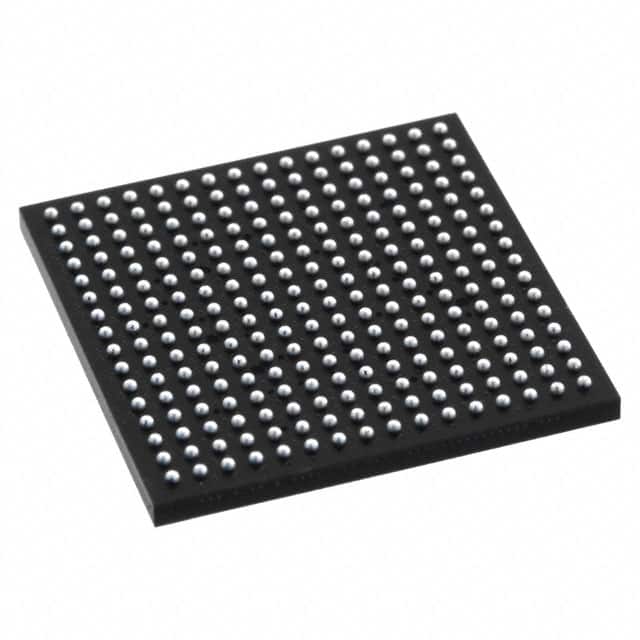
The Lattice Semiconductor LFXP2-17E-6FTN256I is a Field Programmable Gate Array (FPGA) from the XP2 family. It offers 17,000 logic elements and 2,125 LABs, providing significant processing capability. The device includes 282,624 bits of embedded RAM for data storage and manipulation.
With 201 general-purpose input/output pins, this FPGA is designed for flexible system integration. It operates within a voltage range of 1.14V to 1.26V and has an operating temperature range of -40°C to 100°C (TJ). The component is housed in a 256-FTBGA (17x17 mm) package, mounted using a surface mount technique.
This FPGA is suitable for various embedded applications requiring programmable logic. Its specifications support efficient design and implementation in industrial and commercial systems. The device is configured with a 256-LBGA package type.
The LFXP2-17E-6FTN256I has 17,000 logic elements.
The LFXP2-17E-6FTN256I offers 201 I/O pins.
This FPGA has a total of 282,624 bits of embedded RAM.
The operating voltage range is 1.14V to 1.26V.
The operating temperature range is -40°C to 100°C (TJ).
The LFXP2-17E-6FTN256I is supplied in a 256-FTBGA (17x17 mm) package.