

| Distributor | Stock | Pricing | MOQ | PKG | Lead Time | Date Code | On Order Quantity | On Order Delivery | |
|---|---|---|---|---|---|---|---|---|---|
|
9 pcs
|
9 pcs | On Request | 1 | On Request | On Request | 1047 | On Request | On Request |
| Category | |
| Manufacturer Name | |
| Features | |
| Lead Spacing | |
| Mounting Type | |
| Number of I | |
| Number of LABs | |
| Number of Logic Elements | |
| Operating Temperature | |
| Operating Voltage | |
| Supplier Device Package | |
| Tape & Reel | |
| Total RAM Bits | |
| Voltage |
The Lattice Semiconductor LFXP2-17E-6F484C is a Field Programmable Gate Array (FPGA) belonging to the LatticeXP2 family. This device utilizes the flexiFLASH architecture, offering features such as instant-on capability and infinite reconfigurability.
Key electrical specifications include 17,000 logic elements (LUTs) and 2,125 Logic Array Blocks (LABs). It provides 282,624 total RAM bits, with 83 Kbits of distributed RAM and 276 KBits of embedded EBR SRAM across 15 blocks. The device supports up to 358 I/O pins and operates within a voltage range of 1.14V to 1.26V, with a typical operating voltage of 1.2V.
This FPGA is designed for system-level support, compliant with IEEE 1149.1 and IEEE 1532 standards. It includes features like Live Update Technology with secure updates via 128-bit AES encryption and dual-boot capability. The sysDSP block offers high-performance multiply and accumulate functions, with up to 20 18x18 multipliers available.
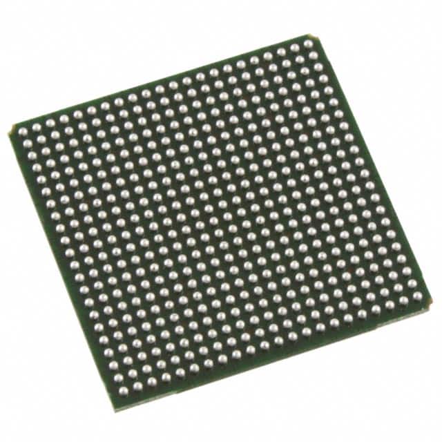
The LFXP2-17E-6F484C comes in a 484-FPBGA (23x23 mm) package, suitable for surface mounting. The operating temperature range is 0°C to 85°C (TJ). The LatticeXP2 family supports various I/O standards including LVCMOS, SSTL, HSTL, PCI, and LVDS.
The LFXP2-17E-6F484C has 17,000 logic elements (LUTs).
The LFXP2-17E-6F484C supports 358 I/O pins.
The operating voltage range for the LFXP2-17E-6F484C is 1.14V to 1.26V.
The LFXP2-17E-6F484C is supplied in a 484-FPBGA (23x23) package.
The LatticeXP2 architecture features flexiFLASH, instant-on capability, infinite reconfigurability, FlashBAK technology, and design security.
Yes, it supports Live Update Technology with secure updates using 128-bit AES encryption and dual-boot capability.