

| Distributor | Stock | Pricing | MOQ | PKG | Lead Time | Date Code | On Order Quantity | On Order Delivery | |
|---|---|---|---|---|---|---|---|---|---|
|
1,016 pcs
|
1016 pcs | On Request | 1 | On Request | On Request | On Request | On Request | On Request |
| Category | |
| Manufacturer Name | |
| Mounting Type | |
| Number of I | |
| Number of LABs | |
| Number of Logic Elements | |
| Operating Temperature | |
| Supplier Device Package | |
| Tape & Reel | |
| Total RAM Bits | |
| Voltage |
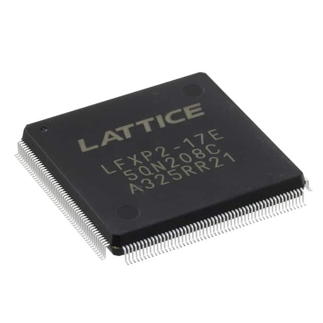
The LFXP2-17E-5QN208I from Lattice Semiconductor is a Field Programmable Gate Array (FPGA) belonging to the LatticeXP2 family. This device is built on a 90nm process and offers 17,000 logic elements and 2,125 LABs, providing substantial capacity for complex digital systems. It features 282,624 RAM bits for embedded memory applications and supports up to 146 I/O pins, enabling versatile system integration.
The operating voltage range for this FPGA is 1.14V to 1.26V, with an operating temperature range of -40°C to 100°C (TJ). The LFXP2-17E-5QN208I is supplied in a 208-pin PQFP package (28x28 mm) and is designed for surface mount applications. It is classified as RoHS3 compliant and has a Moisture Sensitivity Level (MSL) of 1 Unlimited.
This FPGA is suitable for a wide array of applications including telecommunications, industrial automation, consumer electronics, medical devices, and automotive electronics. Its high-density programmable logic and robust I/O capabilities make it a versatile choice for demanding digital designs. Lattice Semiconductor provides development tools such as Lattice Diamond software to support the design process.
The LFXP2-17E-5QN208I FPGA has 17,000 logic elements.
The LFXP2-17E-5QN208I FPGA has a total of 282,624 RAM bits.
The LFXP2-17E-5QN208I FPGA features 146 I/O pins.
The LFXP2-17E-5QN208I FPGA operates within a voltage range of 1.14V to 1.26V.
The LFXP2-17E-5QN208I FPGA is supplied in a 208-pin PQFP (28x28 mm) package.
The operating temperature range for the LFXP2-17E-5QN208I FPGA is -40°C to 100°C (TJ).