

| Distributor | Stock | Pricing | MOQ | PKG | Lead Time | Date Code | On Order Quantity | On Order Delivery | |
|---|---|---|---|---|---|---|---|---|---|
|
168 pcs
|
168 pcs | On Request | 1 | On Request | On Request | On Request | On Request | On Request |
| Category | |
| Manufacturer Name | |
| Lead Spacing | |
| Mounting Type | |
| Number of I | |
| Number of LABs | |
| Number of Logic Elements | |
| Operating Temperature | |
| Package / Case | |
| Supplier Device Package | |
| Tape & Reel | |
| Total RAM Bits | |
| Voltage |
The Lattice Semiconductor LFSC3GA25E-5FFN1020I is a Field Programmable Gate Array (FPGA) from the LatticeSC/M family, specifically the SC series. This device features a high-performance FPGA fabric with 25,000 logic elements and 6,250 LABs, supporting up to 115K LUTs. It offers 476 I/O pins and includes 1.97 Mbits of embedded Block RAM, with speeds up to 500MHz.
This FPGA supports a wide range of electrical characteristics, including an operating voltage range of 0.95V to 1.26V and an operating temperature range of -40°C to 105°C (TJ). It boasts high-speed SERDES capabilities, with 4 to 32 channels supporting performance from 600Mbps to 3.8Gbps, and PURESPEED I/O supporting differential I/O up to 2Gbps DDR. The device also features an extensive clocking network with eight analog PLLs and twelve DLLs.
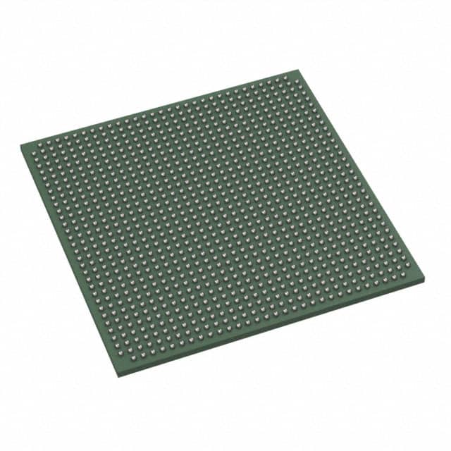
The LFSC3GA25E-5FFN1020I is supplied in a 1020-BBGA, FCBGA package, with a supplier package designation of 1020-OFCBGA (33x33). It is designed for surface mount applications. The device includes features like programmable on-die termination (ODT) and dynamic bit adaptive input logic (AIL) for robust performance. It supports various electrical standards including LVCMOS, SSTL, HSTL, and LVDS variants.
The LFSC3GA25E-5FFN1020I FPGA has 25,000 logic elements.
The LFSC3GA25E-5FFN1020I has 476 I/O pins.
The operating voltage range for the LFSC3GA25E-5FFN1020I is 0.95V to 1.26V.
The LFSC3GA25E-5FFN1020I is supplied in a 1020-BBGA, FCBGA package.
The operating temperature range for the LFSC3GA25E-5FFN1020I is -40°C to 105°C (TJ).
The LFSC3GA25E-5FFN1020I features 1 to 7.8 Mbits of embedded Block RAM.
The high-speed SERDES on this FPGA can reach performance up to 3.8Gbps.