

| Distributor | Stock | Pricing | MOQ | PKG | Lead Time | Date Code | On Order Quantity | On Order Delivery | |
|---|---|---|---|---|---|---|---|---|---|
|
2,000 pcs
|
2000 pcs | On Request | 1 | On Request | On Request | On Request | On Request | On Request |
| Category | |
| Manufacturer Name | |
| Clock Frequency | |
| Mounting Type | |
| Number of I | |
| Number of LABs | |
| Number of Logic Elements | |
| Operating Temperature | |
| Supplier Device Package | |
| Supplier Package | |
| Tape & Reel | |
| Total RAM Bits | |
| Voltage |
The LFSC3GA15E-7FN900C is a Field Programmable Gate Array (FPGA) from Lattice Semiconductor, part of the LatticeSC/M family. This device features a high-performance FPGA fabric with 15,000 Look-Up Tables (LUTs) and supports up to 300 Input/Output (I/O) pins. It operates within a supply voltage range of 0.95V to 1.26V and has a total RAM bit count of 1,054,720.
Key features include a global clock speed of 700MHz and edge clocks up to 1GHz. The FPGA fabric supports 4 to 32 High-Speed SERDES lanes, with performance ranging from 600Mbps to 3.8Gbps. It also incorporates sysMEM™ embedded Block RAM with up to 7.8 Mbits and distributed RAM of up to 1.8 Mbits. The device includes eight analog PLLs and twelve DLLs for advanced clock management.
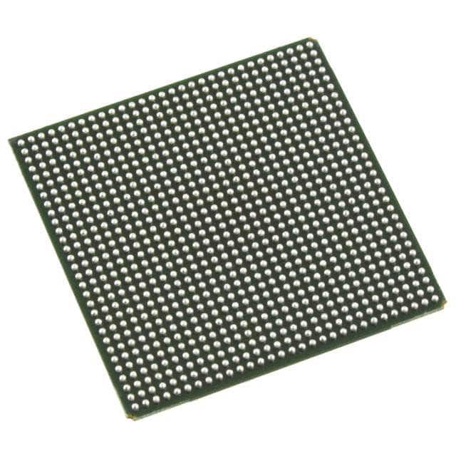
Designed for surface mount applications, the LFSC3GA15E-7FN900C comes in a 900-BBGA package (31x31mm). It operates within a temperature range of 0°C to 85°C (TJ). The FPGA fabric is built on 90nm technology, offering a balance of performance and power efficiency for various embedded applications.
The LFSC3GA15E-7FN900C FPGA has 15,000 logic elements.
The LFSC3GA15E-7FN900C has 300 I/O pins.
The operating voltage range for the LFSC3GA15E-7FN900C is 0.95V to 1.26V.
The LFSC3GA15E-7FN900C is supplied in a 900-BBGA package.
The operating temperature for the LFSC3GA15E-7FN900C is 0°C to 85°C (TJ).
The LFSC3GA15E-7FN900C has a total RAM bit count of 1,054,720 bits.
The maximum SERDES performance of the LFSC3GA15E-7FN900C is 3.8Gbps.