

| Distributor | Stock | Pricing | MOQ | PKG | Lead Time | Date Code | On Order Quantity | On Order Delivery | |
|---|---|---|---|---|---|---|---|---|---|
|
44 pcs
|
44 pcs | On Request | 1 | On Request | On Request | On Request | On Request | On Request |
| Category | |
| Manufacturer Name | |
| Mounting Type | |
| Number of I | |
| Number of I/O | |
| Number of LABs | |
| Number of Logic Elements | |
| Operating Temperature | |
| Operating Voltage | |
| Supplier Device Package | |
| Supplier Package | |
| Total RAM Bits | |
| Voltage |
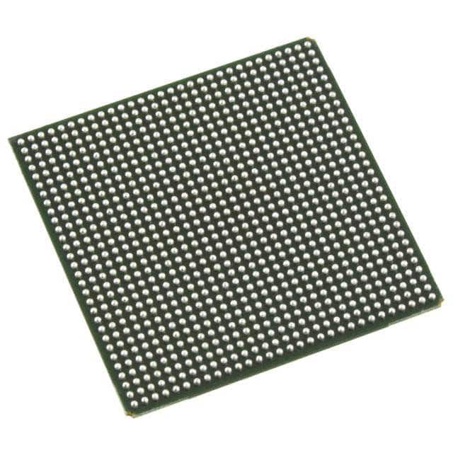
The Lattice Semiconductor LFSC3GA15E-5FN900I is a Field Programmable Gate Array (FPGA) designed for high-performance applications. It offers a substantial fabric with 15,000 logic elements and 3,750 Logic Array Blocks (LABs), complemented by 1.05 Mbits of embedded Block RAM.
This FPGA provides 300 I/O pins and operates within a flexible voltage range of 0.95V to 1.26V. It supports a wide array of electrical standards, including LVCMOS, LVTTL, SSTL, HSTL, PCI, PCI-X, and various differential standards like LVDS and LVPECL. The device is rated for an operating temperature range of -40°C to 105°C (TJ).
Key features include high-speed SERDES capabilities ranging from 600Mbps to 3.8Gbps, a global clock frequency of 700MHz, and edge clocks up to 1GHz. It also supports 2Gbps DDR PURESPEED I/O and single-ended memory interfaces up to 800Mbps. The FPGA is housed in a 900-BBGA package and utilizes a surface mount configuration.
Additional features include programmable on-die termination (ODT), eight analog PLLs, and twelve DLLs for precise clock management. The device also incorporates Masked Array for Cost Optimization (MACO) blocks for system-level integration, low power, and cost efficiency.
The LFSC3GA15E-5FN900I FPGA has 15,000 logic elements.
The operating voltage range for the LFSC3GA15E-5FN900I is 0.95V to 1.26V.
The LFSC3GA15E-5FN900I is supplied in a 900-BBGA package.
The operating temperature range for this FPGA is -40°C to 105°C (TJ).
The LFSC3GA15E-5FN900I features 300 I/O pins.
The LFSC3GA15E-5FN900I has a total of 1,054,720 RAM bits.
The LFSC3GA15E-5FN900I supports LVCMOS 3.3/2.5/1.8/1.5/1.2, LVTTL, SSTL 3/2/18 I, II; HSTL 18/15 I, II, PCI, PCI-X, LVDS, Mini-LVDS, Bus-LVDS, MLVDS, LVPECL, and RSDS.