

| Distributor | Stock | Pricing | MOQ | PKG | Lead Time | Date Code | On Order Quantity | On Order Delivery | |
|---|---|---|---|---|---|---|---|---|---|
|
6 pcs
|
6 pcs | On Request | 1 | On Request | On Request | 615 | On Request | On Request |
| Category | |
| Manufacturer Name | |
| Clock Frequency | |
| Mounting Type | |
| Number of I | |
| Number of Logic Elements | |
| Operating Temperature | |
| Supplier Device Package | |
| Tape & Reel | |
| Total RAM Bits | |
| Voltage |
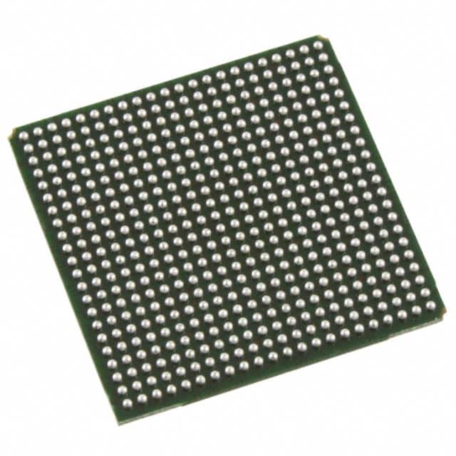
The LFECP33E-5F484C from Lattice Semiconductor Corporation is a Field Programmable Gate Array (FPGA) designed for various embedded applications. This device features 32.8K logic elements and supports up to 360 I/O pins, providing significant flexibility for digital logic implementation.
Key electrical characteristics include an operating voltage range of 1.14V to 1.26V, with a typical value of 1.2V. The FPGA operates at a clock frequency of up to 420 MHz and includes a total memory of 629 kbit, with embedded RAM of 131 kbit and external memory interface RAM of 498 kbit.
Designed for surface mounting, the LFECP33E-5F484C comes in a 484-FPBGA (23x23) package. It operates within a temperature range of 0°C to 70°C (TJ), making it suitable for a range of environmental conditions. The standard package quantity is 300 units, supplied in a tray.
This FPGA is suitable for applications requiring custom digital logic, signal processing, and control functions where programmability and performance are critical.
The LFECP33E-5F484C has 32.8K logic elements.
The LFECP33E-5F484C supports 360 I/O pins.
The operating voltage for the LFECP33E-5F484C is 1.2V.
The LFECP33E-5F484C is supplied in a 484-FPBGA package.
The maximum operating temperature for the LFECP33E-5F484C is +70°C.
The clock frequency of the LFECP33E-5F484C is 420 MHz.