

| Distributor | Stock | Pricing | MOQ | PKG | Lead Time | Date Code | On Order Quantity | On Order Delivery | |
|---|---|---|---|---|---|---|---|---|---|
|
96 pcs
|
96 pcs | On Request | 1 | On Request | On Request | 615 | On Request | On Request |
| Category | |
| Manufacturer Name | |
| Lead Spacing | |
| Mounting Type | |
| Number of I | |
| Number of Logic Elements | |
| Operating Temperature | |
| Package / Case | |
| Supplier Device Package | |
| Tape & Reel | |
| Total RAM Bits | |
| Voltage |
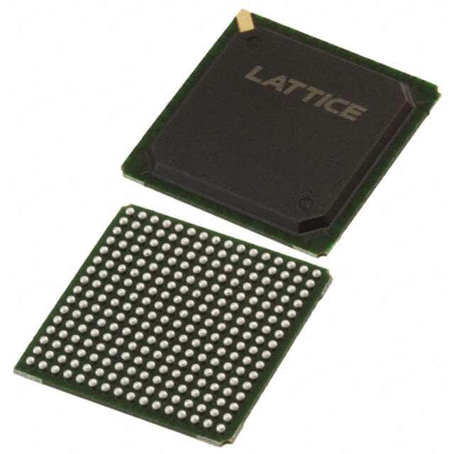
The Lattice Semiconductor LFECP10E-3FN256I is a Field Programmable Gate Array (FPGA) designed for mainstream applications. It offers 10200 logic elements and 195 input/output (I/O) pins, providing significant flexibility for custom digital logic implementation.
This FPGA includes 282624 total RAM bits, supporting embedded and distributed memory configurations. It operates within a supply voltage range of 1.14V to 1.26V and is designed for surface mounting. The operating temperature range is -40°C to 100°C (TJ).
The device is packaged in a 256-FPBGA (17x17) or a 256-BGA, suitable for various board designs. Its specifications make it a versatile component for embedded systems requiring programmable logic capabilities.
The LFECP10E-3FN256I has 10200 logic elements.
The LFECP10E-3FN256I has 195 I/O pins.
The operating voltage range for the LFECP10E-3FN256I is 1.14V to 1.26V.
The LFECP10E-3FN256I is available in a 256-FPBGA (17x17) or 256-BGA package.
The LFECP10E-3FN256I has a total of 282624 RAM bits.
The operating temperature for the LFECP10E-3FN256I is -40°C to 100°C (TJ).