
LFEC3E-4TN144C
Lattice Semiconductor Corporation
The Lattice Semiconductor Corporation LFEC3E-4TN144C is an FPGA with 3100 logic elements and 97 I/O pins. It operates at 1.14V to 1.26V and comes in a 144-TQFP package.


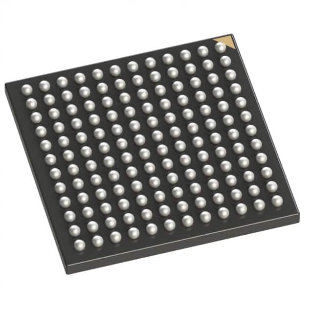
| Distributor | Stock | Pricing | MOQ | PKG | Lead Time | Date Code | On Order Quantity | On Order Delivery | |
|---|---|---|---|---|---|---|---|---|---|
|
5,463 pcs
|
5463 pcs | On Request | 1 | On Request | On Request | 14+ | On Request | On Request | |
|
300 pcs
|
300 pcs | On Request | 1 | On Request | On Request | On Request | On Request | On Request |
| Category | |
| Manufacturer Name | |
| Lead Spacing | |
| Mounting Type | |
| Number of I | |
| Number of Logic Elements | |
| Operating Temperature | |
| Supplier Device Package | |
| Supplier Package | |
| Tape & Reel | |
| Total RAM Bits | |
| Voltage |
The Lattice Semiconductor Corporation LFEC3E-3TN144C is a Field Programmable Gate Array (FPGA) designed for embedded applications. It features 3100 logic elements and 56320 total RAM bits, providing moderate logic capacity suitable for small to mid-size embedded systems.
This FPGA offers 97 input/output pins, supporting a wide range of external device interfacing. The operating supply voltage is between 1.14V and 1.26V, contributing to efficient power usage. The device operates within a junction temperature range of 0°C to 85°C.
The LFEC3E-3TN144C is housed in a 144-TQFP (20x20 mm) package and is designed for surface mounting. This makes it suitable for integration into various PCB designs.
This FPGA is part of the LatticeEC family, optimized for mainstream applications requiring a cost-efficient solution. Its specifications make it useful for custom logic functions, hardware acceleration, and interfacing tasks in industrial controls, automation, and legacy embedded designs.
The LFEC3E-3TN144C FPGA has 3100 logic elements.
The LFEC3E-3TN144C FPGA has 56320 total RAM bits.
The LFEC3E-3TN144C FPGA features 97 I/O pins.
The LFEC3E-3TN144C FPGA operates at a supply voltage of 1.14V to 1.26V.
The LFEC3E-3TN144C FPGA operates within a junction temperature range of 0°C to 85°C.
The LFEC3E-3TN144C FPGA is supplied in a 144-LQFP package.
The LFEC3E-3TN144C FPGA is RoHS3 Compliant.