

| Distributor | Stock | Pricing | MOQ | PKG | Lead Time | Date Code | On Order Quantity | On Order Delivery | |
|---|---|---|---|---|---|---|---|---|---|
|
600 pcs
|
600 pcs | On Request | 1 | On Request | On Request | On Request | On Request | On Request | |
|
45 pcs
|
45 pcs | On Request | 1 | On Request | On Request | 1050 | On Request | On Request |
| Category | |
| Manufacturer Name | |
| Lead Spacing | |
| Mounting Type | |
| Number of I | |
| Number of Logic Elements | |
| Operating Temperature | |
| Operating Voltage | |
| Supplier Device Package | |
| Total RAM Bits | |
| Voltage |
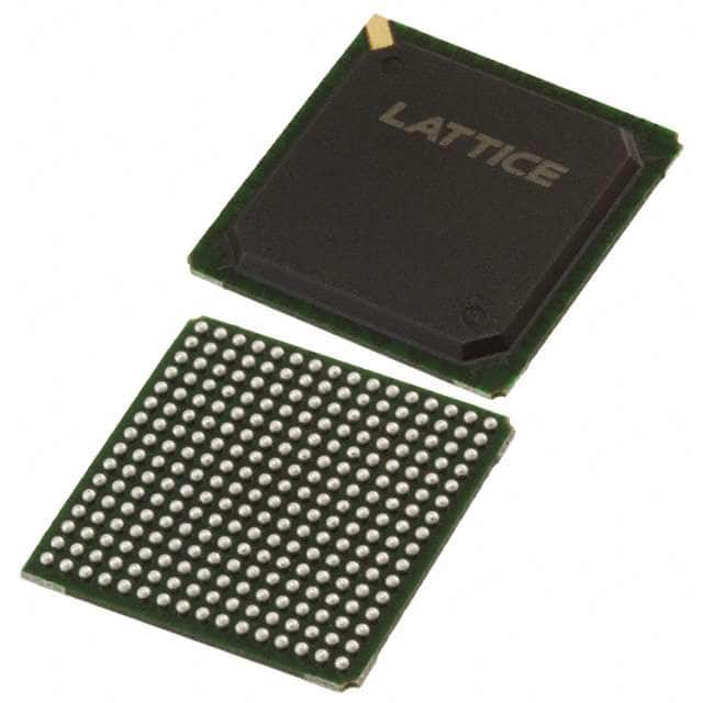
The Lattice Semiconductor LFEC3E-3F256I is a Field Programmable Gate Array (FPGA) designed for embedded applications. It offers 3100 logic elements and 160 input/output pins, providing flexibility for custom hardware designs.
This FPGA includes 56,320 total RAM bits for data storage and operates within a supply voltage range of 1.14V to 1.26V. The operating junction temperature is specified from -40°C to 100°C, making it suitable for a variety of environmental conditions.
The device is designed for surface mounting and comes in a 256-FPBGA package. It is part of the LatticeECP/EC family, known for its balance of features and cost-effectiveness for mainstream applications.
Key electrical specifications include a logic element count of 3100 and 160 I/O pins. The device also supports embedded and distributed memory, with 56,320 total RAM bits available. The operating voltage is 1.14V to 1.26V, and the operating temperature range is -40°C to 100°C.
The LFEC3E-3F256I FPGA features 3100 logic elements, 160 I/O pins, and 56,320 total RAM bits. It operates at a supply voltage of 1.14V to 1.26V.
The operating junction temperature for the LFEC3E-3F256I is -40°C to 100°C.
The LFEC3E-3F256I FPGA is supplied in a 256-FPBGA (17x17) package and is designed for surface mounting.
The RoHS status for the LFEC3E-3F256I is RoHS3 Compliant.
The Moisture Sensitivity Level (MSL) for the LFEC3E-3F256I is 1 Unlimited.