

| Distributor | Stock | Pricing | MOQ | PKG | Lead Time | Date Code | On Order Quantity | On Order Delivery | |
|---|---|---|---|---|---|---|---|---|---|
|
14 pcs
|
14 pcs | On Request | 1 | On Request | On Request | 737 | On Request | On Request |
| Category | |
| Manufacturer Name | |
| Lead Spacing | |
| Mounting Type | |
| Number of I | |
| Number of Logic Elements | |
| Operating Temperature | |
| Supplier Device Package | |
| Tape & Reel | |
| Total RAM Bits | |
| Voltage |
The Lattice Semiconductor LFEC33E-4FN672I is a Field Programmable Gate Array (FPGA) designed for mainstream applications, offering a balance of features and cost-effectiveness. This device boasts 32,800 logic elements (LUTs) and supports up to 496 I/O pins, making it suitable for a wide range of digital logic designs.
Key features include 434,176 total RAM bits, comprising 498 Kbits of embedded block RAM (EBR) and up to 131 Kbits of distributed RAM. It also includes up to four sysCLOCK PLLs for flexible clock management and supports DDR memory interfaces up to DDR400 (200MHz).
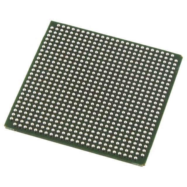
The FPGA operates within a voltage range of 1.14V to 1.26V and has an operating temperature range of -40°C to 100°C (TJ). It is housed in a 672-ball FPBGA package measuring 27x27 mm, designed for surface mounting.
This device is part of the LatticeECP/EC family, known for its extensive density and package options, supporting density migration. It also features flexible I/O buffers supporting various interfaces like LVCMOS, LVTTL, SSTL, HSTL, PCI, and LVDS.
The LFEC33E-4FN672I FPGA has 32800 logic elements.
The LFEC33E-4FN672I has 496 I/O pins.
The operating voltage range for the LFEC33E-4FN672I is 1.14V to 1.26V.
The LFEC33E-4FN672I is supplied in a 672-BBGA package, specifically a 672-FPBGA (27x27) for surface mounting.
The LFEC33E-4FN672I has an operating temperature range of -40°C to 100°C (TJ).
The LFEC33E-4FN672I has a total of 434176 RAM bits.
Yes, the LFEC33E-4FN672I implements DDR memory interfaces up to DDR400 (200MHz).