

| Distributor | Stock | Pricing | MOQ | PKG | Lead Time | Date Code | On Order Quantity | On Order Delivery | |
|---|---|---|---|---|---|---|---|---|---|
|
60 pcs
|
60 pcs | On Request | 1 | On Request | On Request | On Request | On Request | On Request |
| Category | |
| Manufacturer Name | |
| Lead Spacing | |
| Mounting Type | |
| Number of I | |
| Number of LABs | |
| Number of Logic Elements | |
| Operating Temperature | |
| Supplier Device Package | |
| Technology | |
| Total RAM Bits | |
| Voltage |
The Lattice LFE5U-85F-7BG554C is an FPGA belonging to the ECP5/ECP5-5G family, optimized for high performance in economical applications. This device utilizes 40nm technology and offers a capacity of 84,000 logic elements and supports up to 365 user I/O, with this specific part having 259 I/O pins.
Key features include an enhanced DSP architecture, high-speed SERDES (Serializer/Deserializer) capable of up to 5 Gb/s data rates, and high-speed source-synchronous interfaces. The FPGA fabric is designed for high performance with low power and low cost, incorporating reconfigurable SRAM logic, LUT-based logic, distributed and embedded memory, PLLs, DLLs, and advanced configuration support including encryption and dual-boot capabilities. The SERDES functions support protocols like PCI Express, Ethernet, and CPRI.
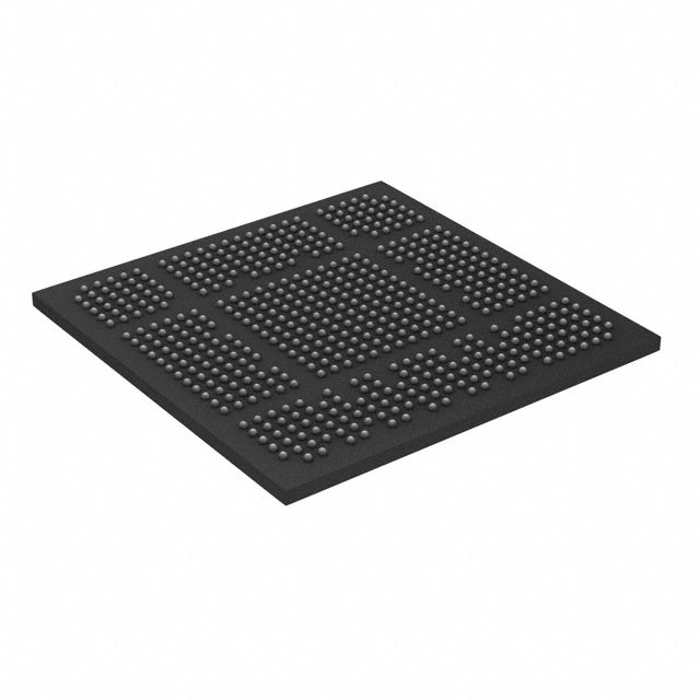
This FPGA is housed in a 554-pin CABGA package and is designed for surface mounting. It operates within a voltage range of 1.045V to 1.155V and has an operating temperature range of 0°C to 85°C (TJ). The ECP5/ECP5-5G family is pin-to-pin compatible with ECP5UM devices, allowing for migration to higher performance designs.
The LFE5U-85F-7BG554C FPGA has 84,000 logic elements.
The LFE5U-85F-7BG554C has 259 I/O pins.
The operating voltage for the LFE5U-85F-7BG554C is between 1.045V and 1.155V.
The LFE5U-85F-7BG554C is supplied in a 554-pin CABGA package.
The operating temperature range is 0°C to 85°C (TJ).
The SERDES data rate can reach up to 5 Gb/s.