

| Distributor | Stock | Pricing | MOQ | PKG | Lead Time | Date Code | On Order Quantity | On Order Delivery | |
|---|---|---|---|---|---|---|---|---|---|
|
447 pcs
|
447 pcs | On Request | 1 | On Request | On Request | On Request | On Request | On Request |
| Category | |
| Manufacturer Name | |
| LUTs | |
| Mounting Type | |
| Number of I | |
| Number of LABs | |
| Number of Logic Elements | |
| Operating Temperature | |
| RAM Size | |
| Supplier Device Package | |
| Total RAM Bits | |
| Voltage |
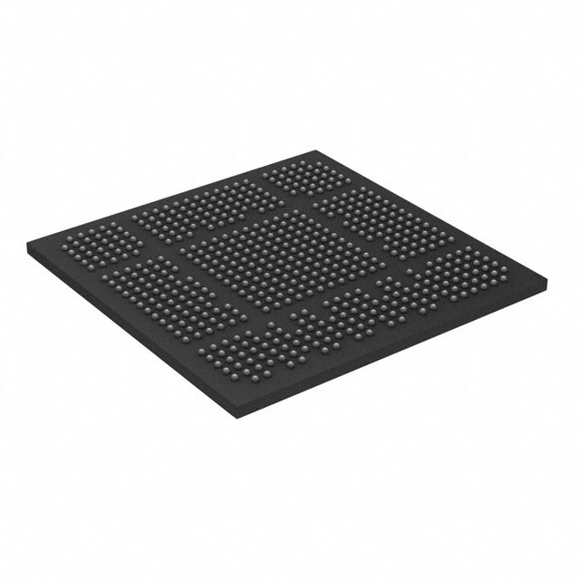
The Lattice Semiconductor LFE5U-85F-6BG554C is a Field Programmable Gate Array (FPGA) from the ECP5 family. This device offers 84,000 logic elements and 21,000 logic array blocks (LABs), providing significant processing power for complex digital designs. It features 259 input/output (I/O) pins, enabling extensive connectivity.
The FPGA includes 468kB of RAM, crucial for data buffering and storage within embedded systems. It operates at a voltage range of 1.045V to 1.155V and is designed for a temperature range of 0°C to 85°C. The device is packaged in a 554-FBGA (554-CABGA) format, suitable for surface mounting.
This component is RoHS3 compliant and has a Moisture Sensitivity Level (MSL) of 1, indicating it is suitable for a wide range of manufacturing environments. Its design makes it applicable in various embedded applications requiring flexible and reconfigurable logic.
The LFE5U-85F-6BG554C has 84000 logic elements.
The LFE5U-85F-6BG554C has 259 I/O pins.
The operating voltage range for the LFE5U-85F-6BG554C is 1.045V to 1.155V.
The LFE5U-85F-6BG554C is supplied in a 554-FBGA package.
The operating temperature range is 0°C to 85°C.