

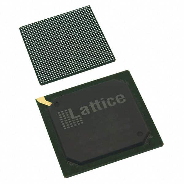
LFE3-95EA-6FN1156I The Lattice Semiconductor LFE3-95EA-6FN1156I is an FPGA with 92,000 logic elements and 490 I/O pins. It features a surface mount package.
Mfr Part #:

LFE3-95EA-6FN1156I

Available from 1 distributors
Mfr Name: Lattice Semiconductor Corporation
Lattice Semiconductor Corporation
The Lattice Semiconductor LFE3-95EA-6FN1156I is an FPGA with 92,000 logic elements and 490 I/O pins. It features a surface mount package.
Total Stock: 30 pcs

LFE3-95EA-6FN1156I Available from 1 distributor

Authorised
Non-Authorised
Distributor Stock Pricing MOQ PKG Lead Time Date Code On Order Quantity On Order Delivery
Non-Authorised Inventory information
30 pcs
30 pcs On Request 1 On Request On Request On Request On Request On Request

LFE3-95EA-6FN1156I Specifications Quick View

Most important parameters for selection – full specs in datasheet.
Category
Manufacturer Name
Lead Spacing
Mounting Type
Number of I
Number of LABs
Number of Logic Elements
Operating Temperature
Supplier Device Package
Total RAM Bits
Voltage

LFE3-95EA-6FN1156I Description

Short technical summary and product information.

The Lattice Semiconductor LFE3-95EA-6FN1156I is a Field Programmable Gate Array (FPGA) from the LatticeECP3 family. It offers a high logic density with 92,000 logic elements and 11,500 LABs, providing ample resources for complex system integration. The device supports up to 490 I/O pins and features flexible memory resources, including up to 4.53 Mbits of embedded block RAM (EBR) and up to 303K bits of distributed RAM.


This FPGA operates at a voltage range of 1.14V to 1.26V and has an operating temperature range of -40°C to 100°C (TJ). It is designed for surface mount applications and comes in a 1156-FPBGA package.


The LatticeECP3 family also includes embedded SERDES capabilities with data rates up to 3.2 Gbps per channel and support for up to 16 channels. It also features sysCLOCK Analog PLLs and DLLs, with up to ten PLLs and two DLLs per device, enabling flexible clock management. The programmable sysI/O buffer supports a wide range of interfaces, including LVTTL, LVCMOS, SSTL, HSTL, LVDS, and more.

LFE3-95EA-6FN1156I Quick Information

Product Type: FPGA
Canonical Name: Lattice Semiconductor Corporation LFE3-95EA-6FN1156I FPGA
Subcategory: Field Programmable Gate Array

LFE3-95EA-6FN1156I Compliance

RoHS Status: RoHS Compliant
Moisture Sensitivity Level (MSL): 1 Unlimited
REACH Status: REACH Unaffected

LFE3-95EA-6FN1156I Features

  • 92,000 logic elements for system integration.
  • 490 I/O pins available for connectivity.
  • Up to 4.53 Mbits embedded block RAM.
  • Supports SERDES up to 3.2 Gbps.
  • Surface mount 1156-FPBGA package.

LFE3-95EA-6FN1156I Applications

  • High-density system integration.
  • Advanced signal processing tasks.
  • High-speed data communication.
  • Embedded system designs.

LFE3-95EA-6FN1156I FAQs

6 frequently asked questions generated from this part’s specifications.
How many logic elements does the LFE3-95EA-6FN1156I FPGA have?

The LFE3-95EA-6FN1156I FPGA has 92,000 logic elements.

What is the total number of I/O pins on this FPGA?

This FPGA features 490 I/O pins.

What is the operating voltage range for the LFE3-95EA-6FN1156I?

The operating voltage range is 1.14V to 1.26V.

What package type is the LFE3-95EA-6FN1156I supplied in?

It is supplied in a 1156-FPBGA (35x35) package.

What are the embedded SERDES data rates supported?

Embedded SERDES data rates range from 150 Mbps to 3.2 Gbps.

How much embedded memory (EBR) is available on this device?

The device offers up to 6.85 Mbits of embedded block RAM (EBR).

Home
Account

Categories