

| Distributor | Stock | Pricing | MOQ | PKG | Lead Time | Date Code | On Order Quantity | On Order Delivery | |
|---|---|---|---|---|---|---|---|---|---|
|
30 pcs
|
30 pcs | On Request | 1 | On Request | On Request | On Request | On Request | On Request |
| Category | |
| Manufacturer Name | |
| Lead Spacing | |
| Mounting Type | |
| Number of I | |
| Number of LABs | |
| Number of Logic Elements | |
| Operating Temperature | |
| Supplier Device Package | |
| Total RAM Bits | |
| Voltage |
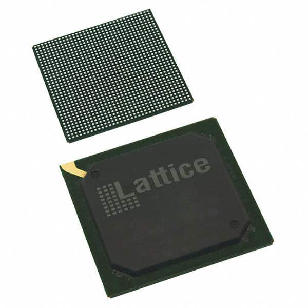
The Lattice Semiconductor LFE3-70EA-8LFN1156C is a Field Programmable Gate Array (FPGA) from the LatticeECP3 family. It offers a logic capacity of 67,000 LUTs and supports up to 490 I/O pins. This device is equipped with 4.53 Mbits of embedded memory and operates within a voltage range of 1.14V to 1.26V.
Key features include a SERDES data rate of up to 3.2 Gbps, up to 16 SERDES channels, and up to 10 PLLs. The FPGA also provides flexible memory resources with up to 303 Kbits of distributed RAM. It supports a wide range of I/O buffer types, including LVTTL, LVCMOS, SSTL, HSTL, LVDS, and more.
The LFE3-70EA-8LFN1156C is designed for surface mount applications and comes in a 1156-FPBGA package. It operates within a temperature range of 0°C to 85°C (TJ). The device also features advanced configuration options such as SPI boot flash, dual-boot capabilities, and 128-bit AES security.
This FPGA is suitable for various applications requiring high logic density, high-speed serial communication, and flexible I/O capabilities.
The LFE3-70EA-8LFN1156C FPGA has a logic capacity of 67,000 LUTs.
The LFE3-70EA-8LFN1156C FPGA supports up to 490 I/O pins.
The operating voltage range for the LFE3-70EA-8LFN1156C FPGA is 1.14V to 1.26V.
The LFE3-70EA-8LFN1156C FPGA is supplied in a 1156-FPBGA (35x35) package.
The operating temperature range for the LFE3-70EA-8LFN1156C FPGA is 0°C to 85°C (TJ).
The FPGA supports a SERDES data rate of up to 3.2 Gbps.
The FPGA offers up to 6.85 Mbits of embedded memory.