

| Distributor | Stock | Pricing | MOQ | PKG | Lead Time | Date Code | On Order Quantity | On Order Delivery | |
|---|---|---|---|---|---|---|---|---|---|
|
4,200 pcs
|
4200 pcs | On Request | 1 | On Request | On Request | 20+ | On Request | On Request | |
|
787 pcs
|
787 pcs | On Request | 1 | On Request | On Request | 20+ | On Request | On Request |
| Category | |
| Manufacturer Name | |
| Failure Rate | |
| Mounting Type | |
| Number of I | |
| Number of LABs | |
| Number of Logic Elements | |
| Operating Temperature | |
| Supplier Device Package | |
| Tape & Reel | |
| Total RAM Bits | |
| Voltage |
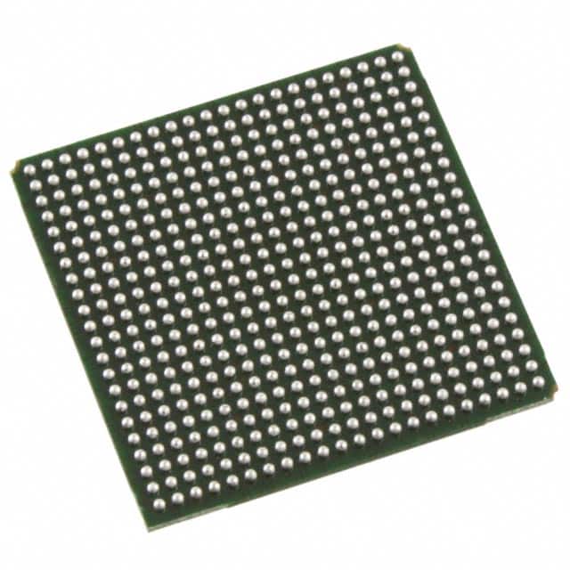
This Lattice Semiconductor LFE3-70EA-8FN484I is a Field Programmable Gate Array (FPGA) from the ECP3 series. It offers a substantial logic density with 67,000 logic elements and 8,375 LABs/CLBs, supported by 4,526,080 total RAM bits. The device provides 295 I/O pins, enabling flexible system integration.
Designed for a 1.14V to 1.26V operating voltage, this FPGA operates within a temperature range of -40°C to 100°C (TJ). It is housed in a 484-BBGA package and requires surface mount installation. The 484-FPBGA (23x23) supplier package details further specify its physical characteristics.
This component is suitable for various embedded applications requiring high logic density and flexible I/O capabilities. Its specifications make it a robust choice for complex digital designs.
The LFE3-70EA-8FN484I FPGA has 67000 logic elements.
The LFE3-70EA-8FN484I FPGA has 295 I/O pins.
The LFE3-70EA-8FN484I FPGA operates within a voltage range of 1.14V to 1.26V.
The LFE3-70EA-8FN484I FPGA is supplied in a 484-BBGA package.
The LFE3-70EA-8FN484I FPGA operates from -40°C to 100°C (TJ).