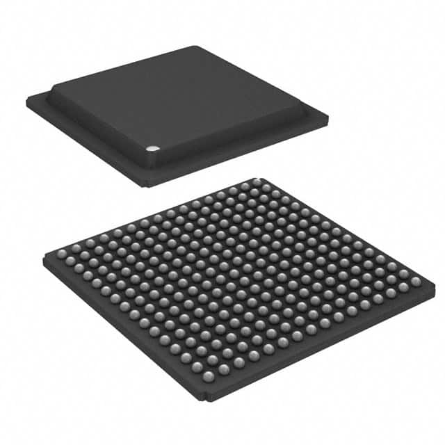
The Lattice Semiconductor LFE3-35EA-8LFTN256I is a Field Programmable Gate Array (FPGA) designed for increased system integration. It features 33,000 logic elements and 4,125 Logic Array Blocks (LABs), providing significant processing power.
This FPGA offers 133 I/O pins and supports a wide range of interfaces through its programmable sysI/O buffer. It includes flexible memory resources with up to 1.36 Mbits of embedded block RAM and 303 Kbits of distributed RAM. The device operates within a voltage range of 1.14V to 1.26V and has an operating temperature range of -40°C to 100°C (TJ).
Designed for surface mount, the LFE3-35EA-8LFTN256I comes in a 256-FTBGA (17x17 mm) package. It supports embedded SERDES with data rates from 150 Mbps to 3.2 Gbps and offers up to 16 channels for protocols like PCI Express and Ethernet. The device also includes sysDSP blocks with up to 160 slices for high-performance multiply and accumulate operations.