

| Distributor | Stock | Pricing | MOQ | PKG | Lead Time | Date Code | On Order Quantity | On Order Delivery | |
|---|---|---|---|---|---|---|---|---|---|
|
377 pcs
|
377 pcs | On Request | 1 | On Request | On Request | On Request | On Request | On Request |
| Category | |
| Manufacturer Name | |
| Lead Spacing | |
| Mounting Type | |
| Number of I | |
| Number of LABs | |
| Number of Logic Elements | |
| Operating Temperature | |
| Supplier Device Package | |
| Supplier Package | |
| Total RAM Bits | |
| Voltage |
The Lattice Semiconductor LFE3-35EA-7FTN256C is a Field Programmable Gate Array (FPGA) from the LatticeECP3 family. It features 33,000 logic elements and 4,125 LABs, offering significant logic density for system integration. The device provides 133 I/O pins and supports a wide range of I/O standards including LVTTL, LVCMOS, SSTL, HSTL, and differential standards.
This FPGA includes flexible memory resources with up to 1.36 Mbits of total RAM bits, comprising embedded block RAM and distributed RAM. It also features embedded SERDES capabilities supporting data rates from 150 Mbps to 3.2 Gbps per channel, with up to 16 channels available for protocols like PCI Express, Ethernet, and Serial RapidIO. The device operates at a core voltage of 1.2V and has an operating temperature range of 0°C to 85°C.
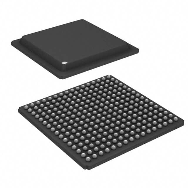
Designed for surface mounting, the LFE3-35EA-7FTN256C comes in a 256-FTBGA (17x17 mm) package. It supports SPI boot flash interface and slave SPI for flexible device configuration. The programmable sysI/O buffer includes on-chip termination and optional equalization filters on inputs.
The LFE3-35EA-7FTN256C FPGA has 33,000 logic elements.
The LFE3-35EA-7FTN256C FPGA has 133 I/O pins.
The operating voltage for the LFE3-35EA-7FTN256C FPGA is between 1.14V and 1.26V.
The LFE3-35EA-7FTN256C FPGA is supplied in a 256-BGA package.
The embedded SERDES data rates supported by this FPGA range from 150 Mbps to 3.2 Gbps.
The LFE3-35EA-7FTN256C has a total of 1.36 Mbits of RAM.