

| Distributor | Stock | Pricing | MOQ | PKG | Lead Time | Date Code | On Order Quantity | On Order Delivery | |
|---|---|---|---|---|---|---|---|---|---|
|
10 pcs
|
10 pcs | On Request | 1 | On Request | On Request | On Request | On Request | On Request |
| Category | |
| Manufacturer Name | |
| Lead Spacing | |
| Mounting Type | |
| Number of I | |
| Number of LABs | |
| Number of Logic Elements | |
| Operating Temperature | |
| Supplier Device Package | |
| Total RAM Bits | |
| Voltage |
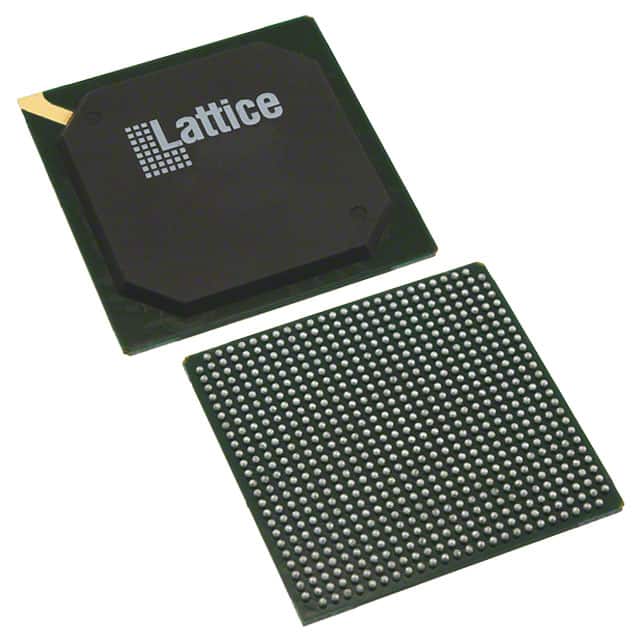
The Lattice LFE3-35EA-6LFN672I is a Field Programmable Gate Array (FPGA) belonging to the LatticeECP3 family. This device offers a substantial logic density with 33,000 logic elements and 4,125 logic array blocks (LABs), providing ample resources for complex digital designs.
Key electrical specifications include 310 I/O pins and 1.36 Mbits of embedded RAM. The operating voltage range is 1.14V to 1.26V, and it operates within a temperature range of -40°C to 100°C (TJ).
This FPGA supports embedded SERDES with data rates up to 3.2 Gbps per channel and can accommodate up to 16 channels. It also features up to 6.85 Mbits of sysMEM™ Embedded Block RAM and up to 303K bits of distributed RAM. The device is housed in a 672-FPBGA (27x27) package and is designed for surface mount applications.
Additional features include up to ten PLLs and two DLLs for clock management. The LatticeECP3 family is known for its high logic density, embedded SERDES capabilities, and flexible memory resources, making it suitable for a wide range of applications requiring high-performance digital processing.
The LFE3-35EA-6LFN672I FPGA has 33,000 logic elements.
The LFE3-35EA-6LFN672I FPGA has 310 I/O pins.
The operating voltage range for the LFE3-35EA-6LFN672I FPGA is 1.14V to 1.26V.
The LFE3-35EA-6LFN672I FPGA is supplied in a 672-FPBGA (27x27) package.
The LFE3-35EA-6LFN672I FPGA operates between -40°C and 100°C (TJ).
The LFE3-35EA-6LFN672I FPGA has a total of 1,358,848 RAM bits.