

| Distributor | Stock | Pricing | MOQ | PKG | Lead Time | Date Code | On Order Quantity | On Order Delivery | |
|---|---|---|---|---|---|---|---|---|---|
|
50 pcs
|
50 pcs | On Request | 1 | On Request | On Request | On Request | On Request | On Request |
| Category | |
| Manufacturer Name | |
| Lead Spacing | |
| Mounting Type | |
| Number of I | |
| Number of LABs | |
| Number of Logic Elements | |
| Operating Temperature | |
| Storage Temperature | |
| Supplier Device Package | |
| Tape & Reel | |
| Total RAM Bits | |
| Voltage |
The Lattice LFE3-17EA-8MG328I is a Field Programmable Gate Array (FPGA) belonging to the LatticeECP3 family. This device offers a logic density of 17,000 Look-Up Tables (LUTs) and 2,125 Logic Array Blocks (LABs), providing significant integration capabilities.
It supports up to 116 I/O pins and features 716,800 total RAM bits, with up to 6.85 Mbits of embedded block RAM and 303 Kbits of distributed RAM. The operating voltage is between 1.14V and 1.26V, with a typical core voltage of 1.2V. The device operates within a temperature range of -40°C to 100°C (TJ).
This FPGA includes embedded SERDES capabilities with data rates up to 3.2 Gbps per channel, supporting various protocols like PCI Express and Ethernet. It also incorporates sysDSP blocks for high-performance multiply and accumulate operations, and sysCLOCK Analog PLLs and DLLs for clock management.
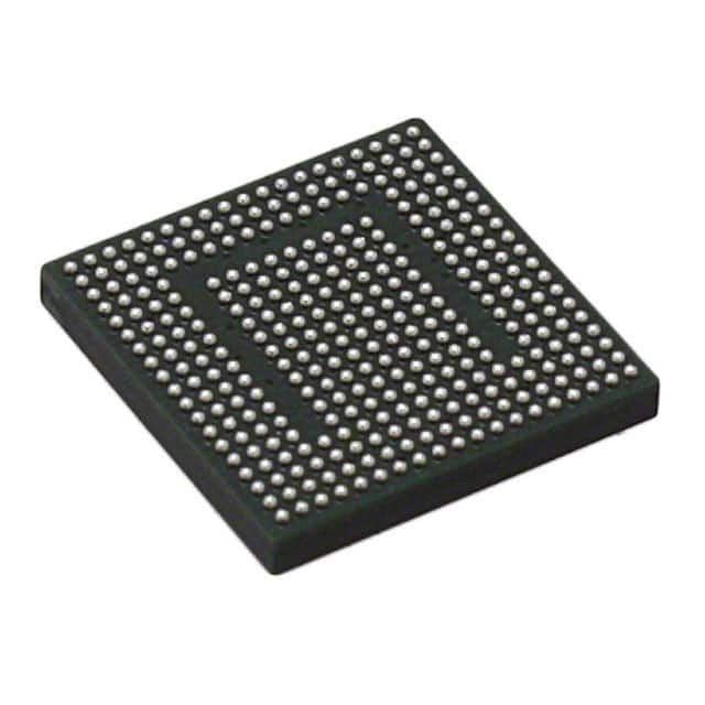
The LFE3-17EA-8MG328I is supplied in a 328-CSBGA (10x10 mm) package, designed for surface mounting. Its flexible I/O buffer supports a wide range of interfaces, including LVTTL, LVCMOS, SSTL, and HSTL.
The LFE3-17EA-8MG328I FPGA has 17,000 logic elements and 2,125 LABs.
The LFE3-17EA-8MG328I FPGA has 116 I/O pins.
The operating voltage for the LFE3-17EA-8MG328I FPGA is between 1.14V and 1.26V.
The LFE3-17EA-8MG328I FPGA is supplied in a 328-CSBGA (10x10 mm) package.
The maximum operating temperature for the LFE3-17EA-8MG328I FPGA is 100°C (TJ).
The embedded SERDES in the LFE3-17EA-8MG328I FPGA supports data rates up to 3.2 Gbps.
The LFE3-17EA-8MG328I FPGA has up to 6.85 Mbits of embedded block RAM.