

| Distributor | Stock | Pricing | MOQ | PKG | Lead Time | Date Code | On Order Quantity | On Order Delivery | |
|---|---|---|---|---|---|---|---|---|---|
|
114 pcs
|
114 pcs | On Request | 1 | On Request | On Request | On Request | On Request | On Request |
| Category | |
| Manufacturer Name | |
| Lead Spacing | |
| Mounting Type | |
| Number of I | |
| Number of LABs | |
| Number of Logic Elements | |
| Operating Temperature | |
| Supplier Device Package | |
| Total RAM Bits | |
| Voltage |
The Lattice Semiconductor LFE3-17EA-7LFTN256C is a Field Programmable Gate Array (FPGA) designed for embedded applications requiring high logic density and I/O connectivity. This device features 17,000 logic elements and 2,125 LABs/CLBs, providing substantial capacity for complex digital designs.
With 133 programmable I/O pins, the LFE3-17EA-7LFTN256C offers flexible interfacing capabilities. It includes 716,800 bits of total RAM, supporting efficient data handling and storage within the FPGA fabric. The device operates within a voltage range of 1.14V to 1.26V, contributing to power efficiency.
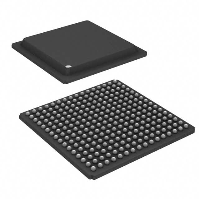
Packaged in a 256-FTBGA (17x17mm) format, this FPGA is designed for surface mounting. It operates reliably within an industrial temperature range of 0°C to 85°C (TJ). The LatticeECP3 family, to which this part belongs, offers features like embedded SERDES, sysDSP, and flexible memory resources.
This FPGA is suitable for applications in industrial automation, network infrastructure, data communications, and signal processing where high performance and configurable logic are essential.
The LFE3-17EA-7LFTN256C features 17,000 logic elements, 2,125 LABs/CLBs, 133 I/O pins, and 716,800 total RAM bits.
The operating voltage is between 1.14V and 1.26V.
The operating temperature range is 0°C to 85°C (TJ).
It is supplied in a 256-FTBGA (17x17mm) package designed for surface mounting.
The Moisture Sensitivity Level is 1.
It is RoHS3 Compliant.