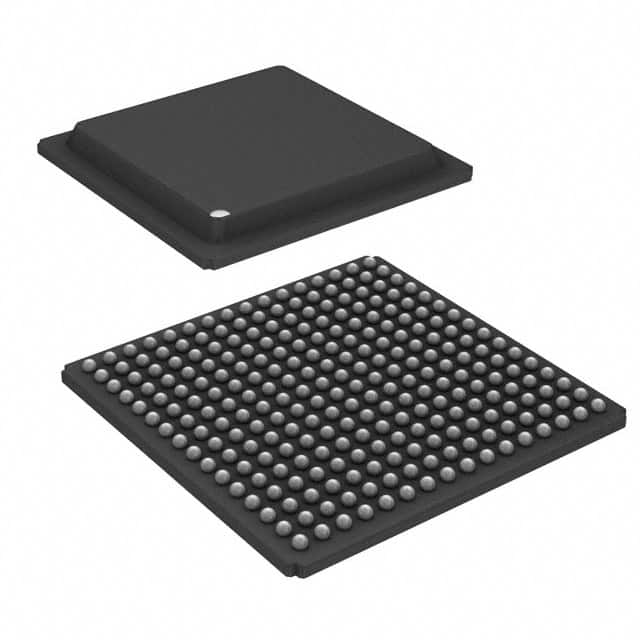
The Lattice Semiconductor LFE3-17EA-6LFTN256I is a Field Programmable Gate Array (FPGA) belonging to the ECP3 series. It offers 17,000 logic elements and 2,125 LABs/CLBs, providing significant logic density for complex designs. The device features 133 programmable I/O pins, enabling high connectivity.
With 716,800 total RAM bits, this FPGA provides ample on-chip memory resources for data handling. It operates within a voltage range of 1.14V to 1.26V and has an industrial operating temperature range of -40°C to 100°C (TJ), ensuring reliable performance in demanding environments. The FPGA is designed for surface mounting and comes in a 256-FTBGA (17x17mm) package.
Key features include embedded SERDES capabilities supporting data rates up to 3.2 Gbps, sysDSP for high-performance multiply and accumulate operations, and flexible memory resources including sysMEM Embedded Block RAM and distributed RAM. The programmable sysI/O buffer supports a wide range of interfaces, and the device includes analog PLLs and DLLs for clock management.