

| Distributor | Stock | Pricing | MOQ | PKG | Lead Time | Date Code | On Order Quantity | On Order Delivery | |
|---|---|---|---|---|---|---|---|---|---|
|
107 pcs
|
107 pcs | On Request | 1 | On Request | On Request | On Request | On Request | On Request |
| Category | |
| Manufacturer Name | |
| Mounting Type | |
| Number of I | |
| Number of LABs | |
| Number of Logic Elements | |
| Operating Temperature | |
| Supplier Device Package | |
| Tape & Reel | |
| Total RAM Bits | |
| Voltage |
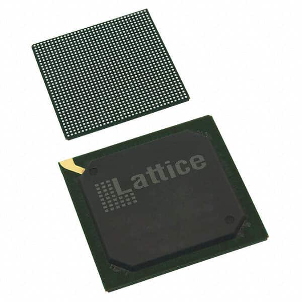
The LFE3-150EA-9FN1156C from Lattice Semiconductor is a high-density Field Programmable Gate Array (FPGA) belonging to the ECP3 series. It is designed for advanced embedded applications requiring significant processing power and flexibility.
This FPGA boasts 149,000 logic elements and 18,625 LABs/CLBs, coupled with 586 I/O pins for extensive interfacing capabilities. It provides 7,014,400 bits of total RAM, enabling complex data buffering and computation tasks. The device operates with a supply voltage ranging from 1.14V to 1.26V and has an operating junction temperature range of 0°C to 85°C.
Packaged in a 1156-BBGA (35x35mm) format, the LFE3-150EA-9FN1156C is designed for surface mounting. Its architecture supports embedded SERDES with data rates up to 3.2 Gbps and includes up to 10 PLLs and 2 DLLs for clock management.
This component is suitable for applications in advanced embedded systems, signal processing, communications, video, networking, and industrial control. It is noted as 'Not For New Designs' but remains suitable for legacy or ongoing systems requiring high-reliability, high-performance environments.
The LFE3-150EA-9FN1156C FPGA has 149,000 logic elements.
The LFE3-150EA-9FN1156C FPGA features 586 I/O pins.
The supply voltage range for the LFE3-150EA-9FN1156C FPGA is 1.14V to 1.26V.
The LFE3-150EA-9FN1156C FPGA is supplied in a 1156-BBGA package.
The operating temperature range for the LFE3-150EA-9FN1156C FPGA is 0°C to 85°C (TJ).
The LFE3-150EA-9FN1156C FPGA has a total of 7,014,400 RAM bits.