

| Distributor | Stock | Pricing | MOQ | PKG | Lead Time | Date Code | On Order Quantity | On Order Delivery | |
|---|---|---|---|---|---|---|---|---|---|
|
150 pcs
|
150 pcs | On Request | 1 | On Request | On Request | On Request | On Request | On Request |
| Category | |
| Manufacturer Name | |
| Mounting Type | |
| Number of I | |
| Number of LABs | |
| Number of Logic Elements | |
| Operating Temperature | |
| Storage Temperature | |
| Supplier Device Package | |
| Tape & Reel | |
| Total RAM Bits | |
| Voltage |
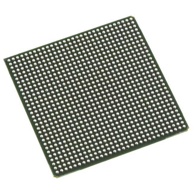
The Lattice Semiconductor LFE2M70E-6FN900I is a Field Programmable Gate Array (FPGA) integrated circuit designed for complex embedded system applications. It offers a substantial logic density with 67,000 logic elements and 8,375 LABs/CLBs, complemented by 4,642,816 total RAM bits for efficient data processing.
This device supports 416 input/output pins and operates within a supply voltage range of 1.14V to 1.26V. The operating temperature range is -40°C to 100°C (TJ), making it suitable for demanding environments. It is housed in a 900-FPBGA (31x31 mm) package and is designed for surface mounting.
The ECP2M series FPGA is ideal for applications requiring flexibility, high-speed data processing, and complex computational tasks. Its extensive RAM and logic cell count enable sophisticated designs in telecommunications, networking hardware, industrial automation, and signal processing systems.
The operating voltage for the LFE2M70E-6FN900I is between 1.14V and 1.26V.
The LFE2M70E-6FN900I has 67,000 logic elements.
This FPGA has a total of 4,642,816 RAM bits.
The operating temperature range is -40°C to 100°C (TJ).
The LFE2M70E-6FN900I is supplied in a 900-FPBGA (31x31 mm) package.