

| Distributor | Stock | Pricing | MOQ | PKG | Lead Time | Date Code | On Order Quantity | On Order Delivery | |
|---|---|---|---|---|---|---|---|---|---|
|
200 pcs
|
200 pcs | On Request | 1 | On Request | On Request | On Request | On Request | On Request |
| Category | |
| Manufacturer Name | |
| AEC Qualified | |
| Automotive Grade | |
| Industrial Grade | |
| LUTs | |
| Lead Spacing | |
| Medical Grade | |
| Military Grade | |
| Mounting Type | |
| Number of I | |
| Number of LABs | |
| Number of Logic Elements | |
| Operating Temperature | |
| Operating Voltage | |
| Supplier Device Package | |
| Tape & Reel | |
| Total RAM Bits | |
| Voltage |
The Lattice Semiconductor Corporation LFE2M70E-6FN1152I is a Field Programmable Gate Array (FPGA) from the ECP2M family. It offers a high logic density with 67,000 logic elements and 8,375 LABs, along with 4,642,816 bits of total RAM.
This FPGA features 436 I/O pins and operates within a voltage range of 1.14V to 1.26V, with a typical supply of 1.2V. The device is designed for a wide operating temperature range of -40°C to 100°C (TJ).
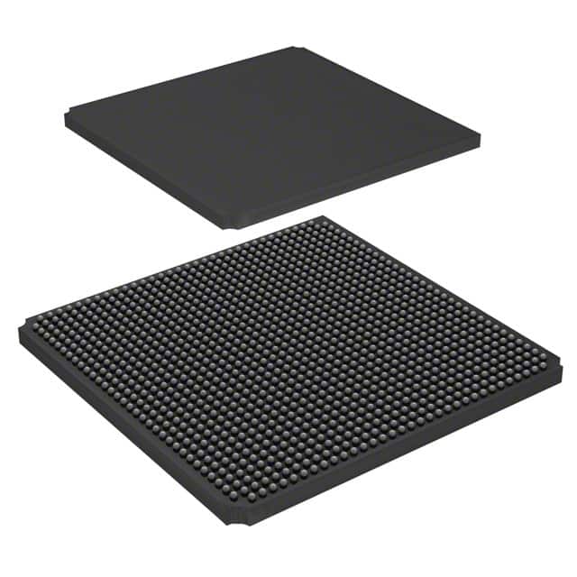
Packaged in a 1152-BBGA (1152-FPBGA, 35x35 mm), the LFE2M70E-6FN1152I is suitable for surface mount applications. The datasheet indicates support for embedded SERDES with data rates up to 3.125 Gbps, sysDSP blocks, and flexible memory resources including sysMEM Embedded Block RAM and distributed RAM.
The LFE2M70E-6FN1152I FPGA has 67,000 logic elements and 8,375 LABs.
The LFE2M70E-6FN1152I FPGA has 436 I/O pins.
The LFE2M70E-6FN1152I FPGA has a total of 4,642,816 bits of RAM.
The LFE2M70E-6FN1152I FPGA operates between 1.14V and 1.26V, with a nominal supply of 1.2V.
The operating temperature range for the LFE2M70E-6FN1152I FPGA is -40°C to 100°C (TJ).
The LFE2M70E-6FN1152I FPGA is supplied in a 1152-BBGA package, measuring 35x35 mm.