

| Distributor | Stock | Pricing | MOQ | PKG | Lead Time | Date Code | On Order Quantity | On Order Delivery | |
|---|---|---|---|---|---|---|---|---|---|
|
240 pcs
|
240 pcs | On Request | 1 | On Request | On Request | On Request | On Request | On Request |
| Category | |
| Manufacturer Name | |
| Lead Spacing | |
| Mounting Type | |
| Number of I | |
| Number of LABs | |
| Number of Logic Elements | |
| Operating Temperature | |
| Supplier Device Package | |
| Tape & Reel | |
| Total RAM Bits | |
| Voltage |
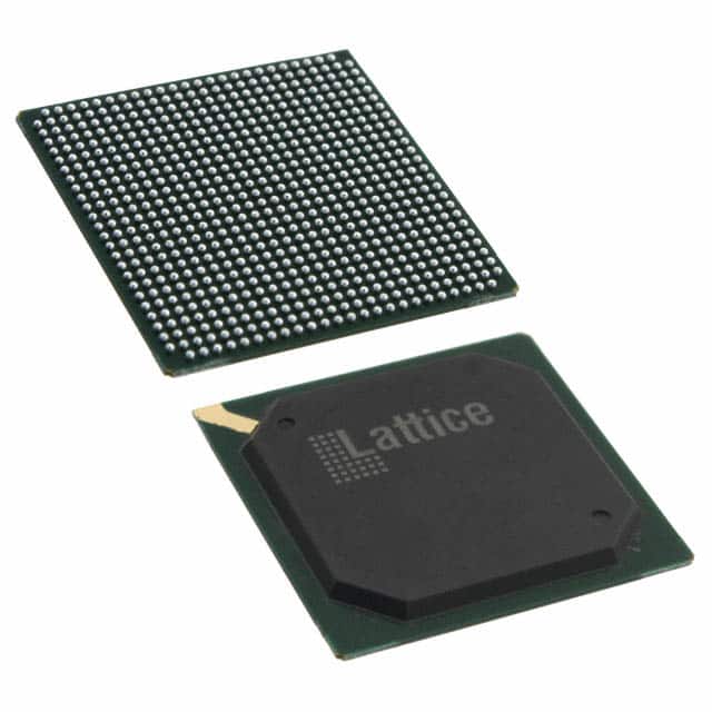
The Lattice Semiconductor LFE2M50SE-6FN672C is a Field Programmable Gate Array (FPGA) designed for high logic density and system integration. It features 48,000 logic elements and 6,000 logic array blocks, providing substantial capacity for complex digital circuitry.
This FPGA offers 4.25 Megabits of total RAM bits for data storage and 372 programmable input/output pins for signal integration. It operates within a supply voltage range of 1.14V to 1.26V and has an operating junction temperature range of 0°C to 85°C.
The device is housed in a 672-FPBGA (27x27mm) package and supports surface mounting. The LatticeECP2M architecture includes features like embedded SERDES, sysDSP blocks, flexible memory resources, and programmable I/O buffers supporting a wide range of interfaces.
Applications for this FPGA include telecom equipment, industrial automation, video processing, medical systems, digital communications, network hardware, and embedded computing, making it suitable for designs requiring extensive customization and high-speed data handling.
The LFE2M50SE-6FN672C FPGA has 48000 logic elements.
The LFE2M50SE-6FN672C features 372 I/O pins.
The operating voltage for the LFE2M50SE-6FN672C is between 1.14V and 1.26V.
The LFE2M50SE-6FN672C is supplied in a 672-FPBGA (27x27) package.
The operating temperature range for the LFE2M50SE-6FN672C is 0°C to 85°C (TJ).
The LFE2M50SE-6FN672C has a total of 4246528 RAM bits.