

| Distributor | Stock | Pricing | MOQ | PKG | Lead Time | Date Code | On Order Quantity | On Order Delivery | |
|---|---|---|---|---|---|---|---|---|---|
|
309 pcs
|
309 pcs | On Request | 1 | On Request | On Request | 1124 | On Request | On Request |
| Category | |
| Manufacturer Name | |
| Failure Rate | |
| Mounting Type | |
| Number of I | |
| Number of LABs | |
| Number of Logic Elements | |
| Operating Temperature | |
| Supplier Device Package | |
| Supplier Package | |
| Total RAM Bits | |
| Voltage |
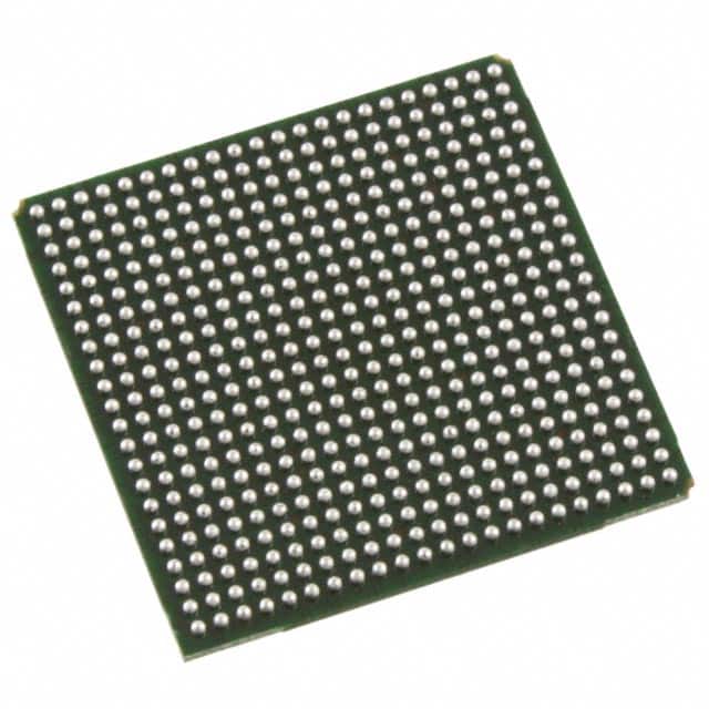
The Lattice Semiconductor LFE2M50E-5F484C is a Field Programmable Gate Array (FPGA) from the ECP2M series. It offers a logic density of 48,000 logic elements and 6,000 LABs, supported by 4,246,528 total RAM bits.
This FPGA provides 270 I/O pins and operates within a voltage range of 1.14V to 1.26V, with a typical operating voltage of 1.2V. The device is designed for surface mounting and comes in a 484-BBGA package, with the supplier package specified as 484-FPBGA (23x23).
Key features include embedded SERDES with data rates from 250 Mbps to 3.125 Gbps, 3 to 42 sysDSP blocks, and flexible memory resources including embedded block RAM (EBR) and distributed RAM. It also supports various analog PLLs and DLLs for clock management. The programmable I/O buffer supports a wide range of interfaces such as LVTTL, LVCMOS, SSTL, HSTL, and differential standards like LVDS and LVPECL. Device configuration options include 1149.1 Boundary Scan compliance, SPI boot flash interface, and dual boot image support.
The LFE2M50E-5F484C FPGA has 48,000 logic elements and 6,000 LABs.
The LFE2M50E-5F484C FPGA has 270 I/O pins.
The LFE2M50E-5F484C FPGA operates between 1.14V and 1.26V, with a typical voltage of 1.2V.
The LFE2M50E-5F484C FPGA is supplied in a 484-BBGA package.
The embedded SERDES in the LFE2M50E-5F484C FPGA supports data rates from 250 Mbps to 3.125 Gbps.
The LFE2M50E-5F484C FPGA offers 55Kbits to 5308Kbits of sysMEM Embedded Block RAM (EBR) and 12K to 202Kbits of distributed RAM.