

| Distributor | Stock | Pricing | MOQ | PKG | Lead Time | Date Code | On Order Quantity | On Order Delivery | |
|---|---|---|---|---|---|---|---|---|---|
|
132 pcs
|
132 pcs | On Request | 1 | On Request | On Request | On Request | On Request | On Request |
| Category | |
| Manufacturer Name | |
| Failure Rate | |
| Mounting Type | |
| Number of I | |
| Number of I/O | |
| Number of LABs | |
| Number of Logic Elements | |
| Operating Temperature | |
| Operating Voltage | |
| Supplier Device Package | |
| Tape & Reel | |
| Total RAM Bits | |
| Voltage |
The Lattice Semiconductor LFE2M35SE-7FN256C is a Field Programmable Gate Array (FPGA) designed for embedded applications requiring high logic density and flexible configuration. This device belongs to the ECP2M series and offers 34,000 logic elements organized into 4,250 LABs/CLBs, providing substantial processing power.
Key electrical specifications include 140 I/O pins for external communication and 2,151,424 total RAM bits for on-chip data storage and buffering. The operating voltage range is 1.14V to 1.26V, with an operating temperature range of 0°C to 85°C (TJ). The FPGA supports embedded SERDES with data rates from 250 Mbps to 3.125 Gbps and up to 16 channels.
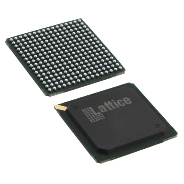
Packaged in a 256-pin Fine Pitch Ball Grid Array (FPBGA) measuring 17x17 mm, the LFE2M35SE-7FN256C is designed for surface mount assembly. Its robust construction and specified operating conditions make it suitable for various demanding electronic systems. The device also features sysDSP blocks and flexible memory resources, including embedded block RAM and distributed RAM.
This FPGA is suitable for complex digital functions and hardware acceleration. Its programmable nature allows for custom logic designs, making it adaptable to a wide range of applications. The device supports various I/O standards and configuration options.
The LFE2M35SE-7FN256C FPGA has 34,000 logic elements and 4,250 LABs/CLBs.
The LFE2M35SE-7FN256C FPGA has 140 I/O pins.
The supply voltage range for the LFE2M35SE-7FN256C FPGA is 1.14V to 1.26V.
The LFE2M35SE-7FN256C FPGA is supplied in a 256-FPBGA (17x17 mm) package.
The operating temperature range for the LFE2M35SE-7FN256C FPGA is 0°C to 85°C (TJ).
The LFE2M35SE-7FN256C FPGA has 2,151,424 total RAM bits.
The embedded SERDES in the LatticeECP2M family supports data rates from 250 Mbps to 3.125 Gbps.