

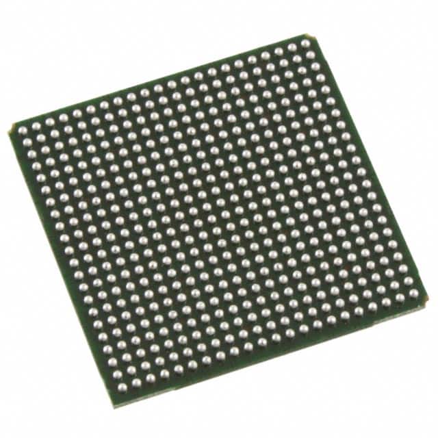
LFE2M35SE-6FN484I The Lattice LFE2M35SE-6FN484I is an FPGA with 34,000 logic elements and 303 I/O pins. It features 2,151,424 total RAM bits and operates within a voltage range of 1.14V to 1.26V.
Mfr Part #:

LFE2M35SE-6FN484I

Available from 1 distributors
Mfr Name: Lattice Semiconductor Corporation
Lattice Semiconductor Corporation
The Lattice LFE2M35SE-6FN484I is an FPGA with 34,000 logic elements and 303 I/O pins. It features 2,151,424 total RAM bits and operates within a voltage range of 1.14V to 1.26V.
✓ Total Stock: 150 pcs

LFE2M35SE-6FN484I Available from 1 distributor

✓ Authorised
✓ Non-Authorised
Distributor Stock Pricing MOQ PKG Lead Time Date Code On Order Quantity On Order Delivery
Non-Authorised Inventory information
150 pcs
150 pcs On Request 1 On Request On Request On Request On Request On Request

LFE2M35SE-6FN484I Specifications Quick View

Most important parameters for selection – full specs in datasheet.
Category
Manufacturer Name
Lead Spacing
Mounting Type
Number of I
Number of LABs
Number of Logic Elements
Operating Temperature
Supplier Device Package
Supplier Package
Total RAM Bits
Voltage

LFE2M35SE-6FN484I Description

Short technical summary and product information.

The Lattice LFE2M35SE-6FN484I is a Field Programmable Gate Array (FPGA) from the LatticeECP2/M family. It offers a high logic density with 34,000 logic elements and 4,250 LABs, supported by 2,151,424 total RAM bits.


This FPGA provides 303 I/O pins and operates at a voltage range of 1.14V to 1.26V. The operating temperature is specified from -40°C to 100°C (TJ). The device supports various features including embedded SERDES with data rates up to 3.125 Gbps, sysDSP blocks, flexible memory resources, and programmable sysI/O buffers supporting a wide range of interfaces.


Packaged in a 484-FPBGA (23x23mm) with surface mount, the LFE2M35SE-6FN484I is designed for system integration. Its configuration options include 1149.1 Boundary Scan compliance and SPI boot flash interface.

LFE2M35SE-6FN484I Quick Information

Product Type: FPGA
Series: LatticeECP2/M
Canonical Name: Lattice LFE2M35SE-6FN484I FPGA
Subcategory: Field Programmable Gate Array

LFE2M35SE-6FN484I Compliance

RoHS Status: RoHS Compliant
Moisture Sensitivity Level (MSL): 1 Unlimited
REACH Status: REACH Unaffected

LFE2M35SE-6FN484I Features

  • 34,000 logic elements for system integration.
  • 303 I/O pins available for connectivity.
  • 2,151,424 total RAM bits for memory.
  • 1.14V to 1.26V operating voltage range.
  • -40°C to 100°C (TJ) operating temperature.

LFE2M35SE-6FN484I Applications

  • High logic density system integration.
  • Embedded SERDES applications.
  • Flexible memory resource designs.
  • Wide range of interface support.

LFE2M35SE-6FN484I FAQs

7 frequently asked questions generated from this part’s specifications.
What is the number of logic elements in the LFE2M35SE-6FN484I FPGA?

The LFE2M35SE-6FN484I FPGA has 34,000 logic elements.

How many I/O pins does the LFE2M35SE-6FN484I FPGA have?

The LFE2M35SE-6FN484I FPGA has 303 I/O pins.

What is the operating voltage for the LFE2M35SE-6FN484I FPGA?

The operating voltage for the LFE2M35SE-6FN484I FPGA is between 1.14V and 1.26V.

What package type is the LFE2M35SE-6FN484I FPGA supplied in?

The LFE2M35SE-6FN484I FPGA is supplied in a 484-FPBGA (23x23mm) package for surface mounting.

What is the operating temperature range for the LFE2M35SE-6FN484I FPGA?

The operating temperature range for the LFE2M35SE-6FN484I FPGA is -40°C to 100°C (TJ).

What are the embedded SERDES capabilities of the Lattice LFE2M35SE-6FN484I?

The Lattice LFE2M35SE-6FN484I features embedded SERDES with data rates from 250 Mbps to 3.125 Gbps, supporting up to 16 channels.

What memory resources are available on the LFE2M35SE-6FN484I FPGA?

The LFE2M35SE-6FN484I FPGA offers 2,151,424 total RAM bits, with sysMEM Embedded Block RAM (EBR) ranging from 55Kbits to 5308Kbits and distributed RAM from 12K to 202Kbits.

Home
Account

Categories