

| Distributor | Stock | Pricing | MOQ | PKG | Lead Time | Date Code | On Order Quantity | On Order Delivery | |
|---|---|---|---|---|---|---|---|---|---|
|
27 pcs
|
27 pcs | On Request | 1 | On Request | On Request | 0939+ | On Request | On Request |
| Category | |
| Manufacturer Name | |
| Lead Spacing | |
| Mounting Type | |
| Number of I | |
| Number of LABs | |
| Number of Logic Elements | |
| Operating Temperature | |
| Supplier Device Package | |
| Tape & Reel | |
| Total RAM Bits | |
| Voltage |
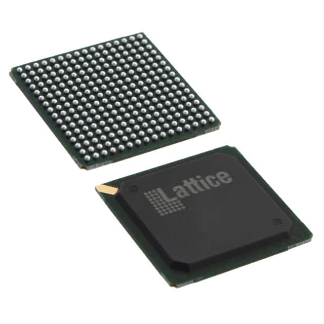
The Lattice LFE2M35E-6FN256C is a Field Programmable Gate Array (FPGA) from the LatticeECP2/M family. It offers a high logic density with 34,000 LUTs (Logic Elements) and supports up to 140 I/O pins.
This FPGA provides flexible memory resources, including 2.15 Mbit of Embedded Block RAM (EBR) and distributed RAM. It features embedded SERDES capabilities with data rates up to 3.125 Gbps and supports various high-speed interfaces like PCI Express and Ethernet.
The device operates within a voltage range of 1.14V to 1.26V and has an operating temperature range of 0°C to 85°C (TJ). It is housed in a 256-FPBGA (17x17) package and is designed for surface mount installation.
Key features include sysDSP blocks for high-performance multiply-accumulate operations, sysCLOCK Analog PLLs and DLLs for clock management, and programmable sysIO buffers supporting a wide array of interfaces.
The LFE2M35E-6FN256C FPGA has 34,000 logic elements.
The LFE2M35E-6FN256C FPGA has 140 I/O pins.
The operating voltage for the LFE2M35E-6FN256C FPGA is between 1.14V and 1.26V.
The LFE2M35E-6FN256C FPGA is supplied in a 256-FPBGA (17x17) package.
The operating temperature range for the LFE2M35E-6FN256C FPGA is 0°C to 85°C (TJ).
The LFE2M35E-6FN256C FPGA has a total of 2,151,424 RAM bits.