

| Distributor | Stock | Pricing | MOQ | PKG | Lead Time | Date Code | On Order Quantity | On Order Delivery | |
|---|---|---|---|---|---|---|---|---|---|
|
10 pcs
|
10 pcs | On Request | 1 | On Request | On Request | 0939+ | On Request | On Request |
| Category | |
| Manufacturer Name | |
| Lead Spacing | |
| Mounting Type | |
| Number of I | |
| Number of LABs | |
| Number of Logic Elements | |
| Operating Temperature | |
| Supplier Device Package | |
| Total RAM Bits | |
| Voltage |
The Lattice Semiconductor LFE2M35E-5FN256I is a Field Programmable Gate Array (FPGA) designed for mid-range embedded system applications requiring moderate logic density. This device offers 34,000 logic elements and 4,250 logic array blocks (LABs/CLBs), providing substantial capacity for complex designs.
Key electrical specifications include 140 general-purpose input/output (I/O) pins for flexible connectivity and a total of 2,151,424 embedded RAM bits. The operating supply voltage ranges from 1.14V to 1.26V, contributing to power efficiency. The device operates within a junction temperature range of -40°C to 100°C.
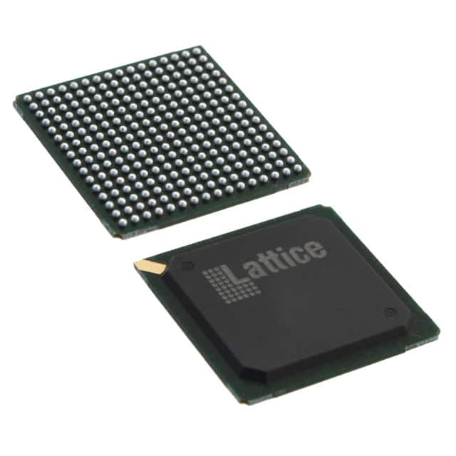
Packaged in a 256-ball Fine-Pitch Ball Grid Array (FPBGA) measuring 17x17 mm, the LFE2M35E-5FN256I is designed for surface mount assembly. This package type is suitable for compact circuit board designs. The FPGA is part of the ECP2M series, known for its performance characteristics in various applications.
This FPGA is suitable for applications such as industrial control systems, communications equipment, embedded computing modules, and consumer electronics requiring programmable logic flexibility. Its moderate logic density and high I/O count make it a versatile choice for mid-tier FPGA implementations.
The LFE2M35E-5FN256I FPGA has 34,000 logic elements.
The LFE2M35E-5FN256I FPGA has 140 I/O pins.
The operating voltage range for the LFE2M35E-5FN256I FPGA is 1.14V to 1.26V.
The LFE2M35E-5FN256I FPGA is supplied in a 256-FPBGA (17x17 mm) package.
The operating temperature range for the LFE2M35E-5FN256I FPGA is -40°C to 100°C (TJ).