

| Distributor | Stock | Pricing | MOQ | PKG | Lead Time | Date Code | On Order Quantity | On Order Delivery | |
|---|---|---|---|---|---|---|---|---|---|
|
300 pcs
|
300 pcs | On Request | 1 | On Request | On Request | On Request | On Request | On Request |
| Category | |
| Manufacturer Name | |
| Lead Spacing | |
| Mounting Type | |
| Number of I | |
| Number of LABs | |
| Number of Logic Elements | |
| Operating Temperature | |
| Supplier Device Package | |
| Supplier Package | |
| Tape & Reel | |
| Total RAM Bits | |
| Voltage |
The Lattice Semiconductor LFE2M100E-6FN1152I is a Field Programmable Gate Array (FPGA) from the ECP2M series. It offers a high logic density with 95,000 logic elements and 11,875 logic array blocks (LABs). This device provides 520 input/output (I/O) pins and features 5.43 Mbits of embedded RAM.
Designed for system integration, the LFE2M100E-6FN1152I supports a wide range of interfaces through its programmable sysIO buffer, including LVTTL, LVCMOS, SSTL, HSTL, and various differential standards like LVDS and LVPECL. It operates within a voltage supply range of 1.14V to 1.26V and has an operating temperature range of -40°C to 100°C (TJ).
The FPGA includes embedded SERDES capabilities with data rates up to 3.125 Gbps and supports up to 16 channels. It also features sysDSP blocks for high-performance multiply and accumulate operations, and sysCLOCK Analog PLLs and DLLs for flexible clock management. The device is configured using a 1149.1 Boundary Scan compliant interface and supports SPI boot flash.
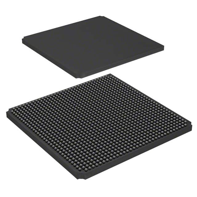
This FPGA is available in a 1152-BBGA package, specifically a 1152-FPBGA (35x35) supplier package, and is designed for surface mounting.
The LFE2M100E-6FN1152I FPGA has 95,000 logic elements.
The LFE2M100E-6FN1152I FPGA has 520 I/O pins.
The operating voltage range for the LFE2M100E-6FN1152I FPGA is 1.14V to 1.26V.
The LFE2M100E-6FN1152I FPGA is supplied in a 1152-BBGA package.
The operating temperature range for the LFE2M100E-6FN1152I FPGA is -40°C to 100°C (TJ).
The LFE2M100E-6FN1152I FPGA supports embedded SERDES data rates from 250 Mbps to 3.125 Gbps.
The LFE2M100E-6FN1152I FPGA has 5.43 Mbits of embedded RAM.