

| Distributor | Stock | Pricing | MOQ | PKG | Lead Time | Date Code | On Order Quantity | On Order Delivery | |
|---|---|---|---|---|---|---|---|---|---|
|
2,542 pcs
|
2542 pcs | On Request | 1 | On Request | On Request | On Request | On Request | On Request |
| Category | |
| Manufacturer Name | |
| Memory Size | |
| Mounting Type | |
| Number of I | |
| Number of LABs | |
| Number of Logic Elements | |
| Number of Pins | |
| Operating Temperature | |
| Operating Voltage | |
| RAM Size | |
| Supplier Device Package | |
| Supplier Package | |
| Tape & Reel | |
| Total RAM Bits | |
| Voltage |
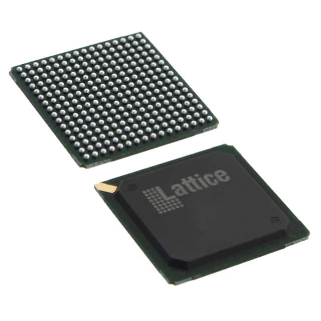
The Lattice Semiconductor LFE2-6SE-6FN256C is a Field Programmable Gate Array (FPGA) from the LatticeECP2 family, specifically the S-Series. This device offers a logic density of 6K LUTs (Look-Up Tables) and provides 190 I/O pins for interfacing.
Key electrical specifications include an operating voltage range of 1.14V to 1.26V, with a nominal operating voltage of 1.2V. It features a maximum operating frequency of 357MHz and includes 750 Logic Array Blocks (LABs) and 6000 logic elements. The device also offers 56320 bits of total RAM.
This FPGA is designed for surface mount applications and comes in a 256-BGA package, specifically a 256-FPBGA measuring 17x17 mm. The operating temperature range is from 0°C to 85°C (TJ). It is RoHS3 compliant and has a Moisture Sensitivity Level (MSL) of 1.
This component is suitable for various embedded system designs requiring flexible logic implementation and I/O connectivity.
The LFE2-6SE-6FN256C FPGA has a logic density of 6K LUTs.
The LFE2-6SE-6FN256C FPGA has 190 I/O pins.
The operating voltage for the LFE2-6SE-6FN256C FPGA is between 1.14V and 1.26V, with a typical value of 1.2V.
The LFE2-6SE-6FN256C FPGA is supplied in a 256-FPBGA (17x17) package.
The maximum operating temperature for the LFE2-6SE-6FN256C FPGA is 85°C (TJ).
The LFE2-6SE-6FN256C FPGA has a maximum frequency of 357MHz.
The LFE2-6SE-6FN256C FPGA is RoHS3 Compliant.