

| Distributor | Stock | Pricing | MOQ | PKG | Lead Time | Date Code | On Order Quantity | On Order Delivery | |
|---|---|---|---|---|---|---|---|---|---|
|
2,000 pcs
|
2000 pcs | On Request | 1 | On Request | On Request | On Request | On Request | On Request |
| Category | |
| Manufacturer Name | |
| Mounting Type | |
| Number of I | |
| Number of I/O | |
| Number of LABs | |
| Number of Logic Elements | |
| Operating Temperature | |
| Supplier Device Package | |
| Tape & Reel | |
| Total RAM Bits | |
| Voltage |
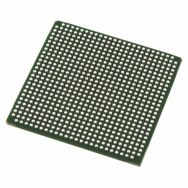
The Lattice Semiconductor LFE2-35E-6FN672C is a Field Programmable Gate Array (FPGA) designed for complex digital logic applications. It offers a substantial logic density with 32,000 logic cells and 4,000 LABs/CLBs, complemented by 339,968 total RAM bits for flexible memory configurations.
This FPGA provides 450 I/O pins, enabling extensive system connectivity. It operates within a supply voltage range of 1.14V to 1.26V and is designed for a temperature range of 0°C to 85°C (TJ). The device is housed in a 672-FPBGA (27x27mm) package, suitable for surface mounting.
Part of the ECP2 series, this FPGA is built on a non-volatile architecture and utilizes a fine-pitch ball grid array for dense board designs. Its specifications make it suitable for applications requiring high integration, temperature resilience, and programmable logic flexibility, such as industrial control systems, embedded system boards, and network equipment.
The LFE2-35E-6FN672C FPGA has 32,000 logic elements.
The LFE2-35E-6FN672C features 339,968 total RAM bits.
The LFE2-35E-6FN672C FPGA provides 450 I/O pins.
The LFE2-35E-6FN672C operates within a supply voltage range of 1.14V to 1.26V.
The operating temperature range for the LFE2-35E-6FN672C is 0°C to 85°C (TJ).
The LFE2-35E-6FN672C is supplied in a 672-FPBGA (27x27mm) package.