

| Distributor | Stock | Pricing | MOQ | PKG | Lead Time | Date Code | On Order Quantity | On Order Delivery | |
|---|---|---|---|---|---|---|---|---|---|
|
30 pcs
|
30 pcs | On Request | 1 | On Request | On Request | On Request | On Request | On Request |
| Category | |
| Manufacturer Name | |
| Lead Spacing | |
| Mounting Type | |
| Number of I | |
| Number of I/O | |
| Number of LABs | |
| Number of Logic Elements | |
| Operating Temperature | |
| Supplier Device Package | |
| Total RAM Bits | |
| Voltage |
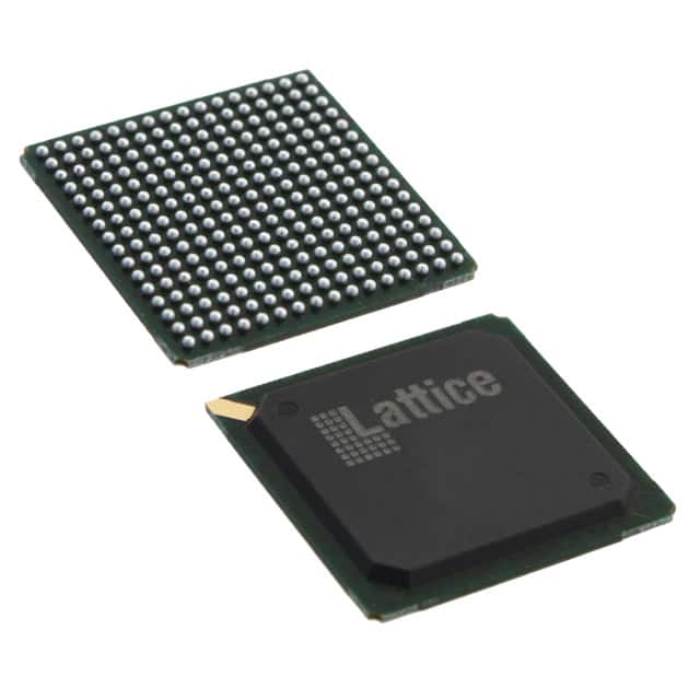
The Lattice Semiconductor LFE2-20SE-7FN256C is a Field Programmable Gate Array (FPGA) designed for system integration. It offers a logic density of 21000 logic elements and 2625 LABs, supported by 282624 bits of embedded RAM.
This FPGA provides 193 I/O pins and operates within a voltage range of 1.14V to 1.26V. The device is specified for an operating junction temperature range of 0°C to 85°C. It is designed for surface mounting and comes in a 256-BGA package.
The LatticeECP2/M family, to which this device belongs, features embedded SERDES, sysDSP blocks, flexible memory resources, and programmable I/O buffers supporting a wide range of interfaces.
The LFE2-20SE-7FN256C FPGA has 21000 logic elements and 2625 LABs.
The LFE2-20SE-7FN256C FPGA has 193 I/O pins.
The operating voltage for the LFE2-20SE-7FN256C FPGA is between 1.14V and 1.26V.
The LFE2-20SE-7FN256C FPGA is supplied in a 256-BGA package.
The operating temperature range for the LFE2-20SE-7FN256C FPGA is 0°C to 85°C (TJ).