

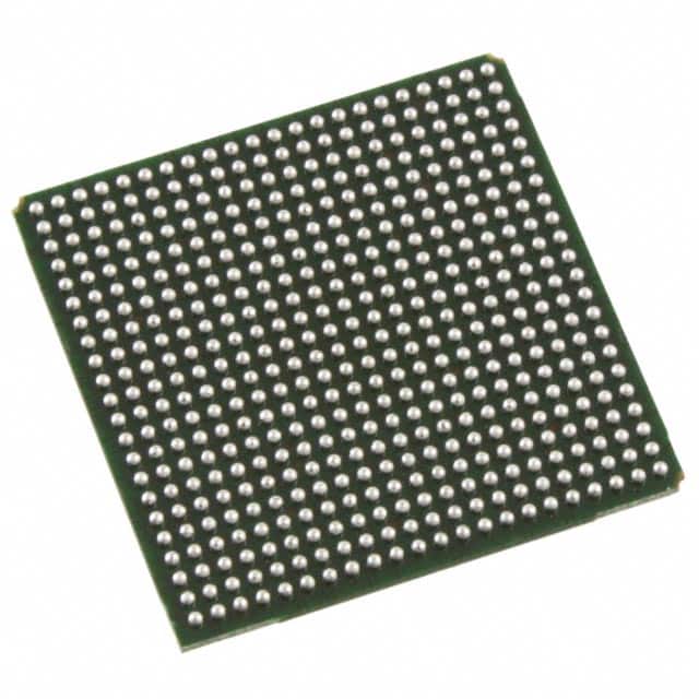
LFE2-12E-5F484C The Lattice Semiconductor LFE2-12E-5F484C is an FPGA with 12000 logic elements and 297 I/O pins. It features 226304 total RAM bits and operates from 1.14V to 1.26V.
Mfr Part #:

LFE2-12E-5F484C

Available from 1 distributors
Mfr Name: Lattice Semiconductor Corporation
Lattice Semiconductor Corporation
The Lattice Semiconductor LFE2-12E-5F484C is an FPGA with 12000 logic elements and 297 I/O pins. It features 226304 total RAM bits and operates from 1.14V to 1.26V.
✓ Total Stock: 10 pcs

LFE2-12E-5F484C Available from 1 distributor

✓ Authorised
✓ Non-Authorised
Distributor Stock Pricing MOQ PKG Lead Time Date Code On Order Quantity On Order Delivery
Non-Authorised Inventory information
10 pcs
10 pcs On Request 1 On Request On Request On Request On Request On Request

LFE2-12E-5F484C Specifications Quick View

Most important parameters for selection – full specs in datasheet.
Category
Manufacturer Name
Lead Spacing
Mounting Type
Number of I
Number of LABs
Number of Logic Elements
Operating Temperature
Supplier Device Package
Tape & Reel
Total RAM Bits
Voltage

LFE2-12E-5F484C Description

Short technical summary and product information.

The Lattice Semiconductor LFE2-12E-5F484C is a Field Programmable Gate Array (FPGA) from the ECP2 series. It offers a logic density of 12000 logic elements and 1500 LABs, supported by 297 I/O pins. This device provides 226304 bits of total RAM.


Designed for system integration, the LFE2-12E-5F484C operates within a voltage range of 1.14V to 1.26V and has an operating temperature range of 0°C to 85°C (TJ). It is housed in a 484-BBGA package, specifically a 484-FPBGA (23x23) variant, and is designed for surface mounting.


Key features include its substantial logic capacity and integrated memory resources, making it suitable for various embedded applications requiring flexible and high-performance digital processing. The device supports a wide range of interfaces through its programmable I/O buffers.

LFE2-12E-5F484C Quick Information

Product Type: FPGA
Series: ECP2
Canonical Name: Lattice Semiconductor LFE2-12E-5F484C FPGA
Subcategory: Field Programmable Gate Array

LFE2-12E-5F484C Compliance

RoHS Status: RoHS Compliant
Moisture Sensitivity Level (MSL): 1 Unlimited
REACH Status: REACH Unaffected

LFE2-12E-5F484C Features

  • 12000 logic elements and 1500 LABs
  • 297 I/O pins available
  • 226304 total RAM bits
  • 1.14V to 1.26V operating voltage
  • Surface mount 484-BBGA package

LFE2-12E-5F484C Applications

  • Suitable for system integration
  • Flexible embedded processing needs
  • High-performance digital logic
  • Wide range of interface support

LFE2-12E-5F484C FAQs

5 frequently asked questions generated from this part’s specifications.
What is the number of logic elements in the LFE2-12E-5F484C?

The LFE2-12E-5F484C has 12000 logic elements.

How many I/O pins does the LFE2-12E-5F484C have?

The LFE2-12E-5F484C has 297 I/O pins.

What is the operating voltage range for the LFE2-12E-5F484C?

The operating voltage range for the LFE2-12E-5F484C is 1.14V to 1.26V.

What package type is the LFE2-12E-5F484C supplied in?

The LFE2-12E-5F484C is supplied in a 484-BBGA package, specifically a 484-FPBGA (23x23).

What is the operating temperature range for the LFE2-12E-5F484C?

The operating temperature range for the LFE2-12E-5F484C is 0°C to 85°C (TJ).

Home
Account

Categories