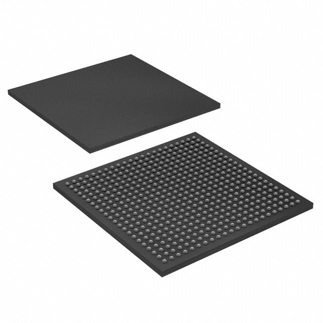
The Lattice Semiconductor LFCPNX-100-8BBG484I is a Field Programmable Gate Array (FPGA) designed for various embedded applications. This device features 96,000 logic elements and 24,000 logic array blocks (LABs), providing significant processing capabilities.
It offers 313 input/output (I/O) pins, allowing for extensive connectivity. The operating voltage range is between 0.95V and 1.05V, with an operating temperature range of -40°C to 100°C (TJ). The total RAM bits available are 3,833,856.
This FPGA comes in a 484-LFBGA package, with a supplier device package specified as 484-CABGA (19x19). It is designed for surface mount applications. The device is described as RoHS3 Compliant, with an MSL rating of 1 Unlimited, and REACH Unaffected.