
LCMXO3L-9400E-6BG256C
Lattice Semiconductor Corporation
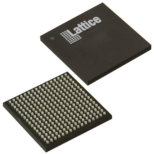
The Lattice Semiconductor LCMXO3L-9400E-6BG256C is an FPGA with 9400 logic elements and 206 I/O pins. It operates within a voltage range of 1.14V to 1.26V.


| Distributor | Stock | Pricing | MOQ | PKG | Lead Time | Date Code | On Order Quantity | On Order Delivery | |
|---|---|---|---|---|---|---|---|---|---|
|
30 pcs
|
30 pcs | On Request | 1 | On Request | On Request | On Request | On Request | On Request |
| Category | |
| Manufacturer Name | |
| Lead Spacing | |
| Mounting Type | |
| Number of I | |
| Number of LABs | |
| Number of Logic Elements | |
| Operating Temperature | |
| Supplier Device Package | |
| Total RAM Bits | |
| Voltage |
The Lattice Semiconductor LCMXO3LF-9400E-6BG256C is a Field Programmable Gate Array (FPGA) designed for embedded applications. It features 9400 logic elements and 1175 logic array blocks, providing significant flexibility for digital functions. The device includes 442,368 bits of total RAM.
This FPGA offers 206 programmable I/O pins, supporting a wide range of interface requirements. It operates with a supply voltage between 1.14V and 1.26V and has an operating temperature range of 0°C to 85°C (TJ). The component is housed in a 256-CABGA (14x14) package, suitable for surface mounting.
Ideal for applications requiring flexible logic implementation and system connectivity, such as consumer electronics, industrial control, and communication equipment. Its non-volatile flash technology ensures reliable configuration and rapid power-up. The device is RoHS3 compliant and REACH unaffected.
The LCMXO3LF-9400E-6BG256C FPGA has 9400 logic elements.
The LCMXO3LF-9400E-6BG256C offers 206 I/O pins.
The operating voltage range for the LCMXO3LF-9400E-6BG256C is 1.14V to 1.26V.
The LCMXO3LF-9400E-6BG256C is supplied in a 256-CABGA (14x14) package.
The operating temperature range for this FPGA is 0°C to 85°C (TJ).