| Distributor | Stock | Pricing | MOQ | PKG | Lead Time | Date Code | On Order Quantity | On Order Delivery | |
|---|---|---|---|---|---|---|---|---|---|
|
3,466 pcs
|
3466 pcs | On Request | 1 | On Request | On Request | On Request | On Request | On Request | |
|
841 pcs
|
841 pcs | On Request | 1 | On Request | On Request | On Request | On Request | On Request |
| Category | |
| Manufacturer Name | |
| Lead Spacing | |
| Mounting Type | |
| Number of I | |
| Number of LABs | |
| Number of Logic Elements | |
| Operating Temperature | |
| Supplier Device Package | |
| Total RAM Bits | |
| Voltage |
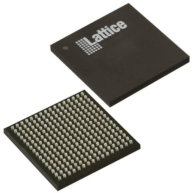
The Lattice Semiconductor LCMXO3LF-9400C-6BG256C is a MachXO3LF FPGA designed for control PLD and bridging applications. It offers a logic density of 9400 LUTs and 206 user I/O pins, making it suitable for complex glue logic and board management tasks.
This FPGA provides 442,368 total RAM bits, including 73 kbit of distributed RAM and 432 kbit of block RAM. It features 2 PLLs for clock management and hardened blocks for I2C, SPI, Timer/Counter, and Oscillator functions. The device operates within a supply voltage range of 2.375V to 3.465V and has an operating temperature range of 0°C to 85°C (TJ).
The LCMXO3LF-9400C-6BG256C is supplied in a 256-LFBGA package and supports surface mount. Its non-volatile, instant-on configuration allows for fast and predictable system bring-up. The device is programmable via JTAG, SPI, or I2C interfaces.

The LCMXO3LF-9400C-6BG256C FPGA has a logic density of 9400 LUTs.
The LCMXO3LF-9400C-6BG256C has 206 user I/O pins.
The operating voltage range for the LCMXO3LF-9400C-6BG256C is 2.375V to 3.465V.
The LCMXO3LF-9400C-6BG256C is supplied in a 256-LFBGA package.
The operating temperature for the LCMXO3LF-9400C-6BG256C is 0°C to 85°C (TJ).
Yes, the LCMXO3LF-9400C-6BG256C features 2x I2C and 1x SPI hardened blocks.
The UFM memory size for the LCMXO3LF-9400C-6BG256C is 448 kbit.