

| Distributor | Stock | Pricing | MOQ | PKG | Lead Time | Date Code | On Order Quantity | On Order Delivery | |
|---|---|---|---|---|---|---|---|---|---|
|
3,421 pcs
|
3421 pcs | On Request | 1 | On Request | On Request | On Request | On Request | On Request |
| Category | |
| Manufacturer Name | |
| Lead Spacing | |
| Mounting Type | |
| Number of I | |
| Number of LABs | |
| Number of Logic Elements | |
| Operating Temperature | |
| Package / Case | |
| Supplier Device Package | |
| Total RAM Bits | |
| Voltage |
The Lattice Semiconductor LCMXO3LF-4300C-6BG324I is a Field Programmable Gate Array (FPGA) designed for various embedded applications. This device offers 4320 logic elements and 540 logic array blocks, providing significant processing capability.
Key electrical specifications include an operating voltage range of 2.375V to 3.465V and 279 input/output pins. The FPGA has a total RAM bit count of 94208. It is designed to operate reliably within a temperature range of -40°C to 100°C (TJ).
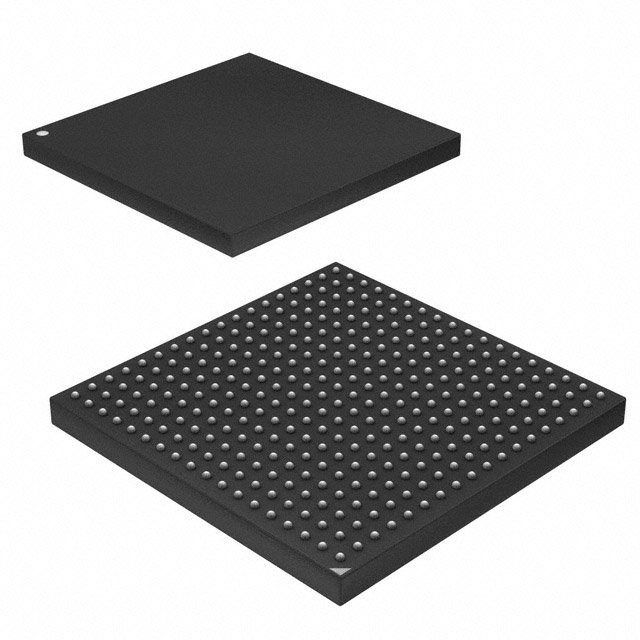
The component is housed in a 324-CABGA package, measuring 15x15, and utilizes a Surface Mount mounting type. The package type is specified as 324-LFBGA. This FPGA is suitable for applications requiring flexible logic implementation and high-speed data processing.
Compliance information indicates RoHS3 compliance, an MSL of 1 (Unlimited), and REACH Unaffected status. These attributes are based on available database information and should be reviewed for specific application requirements.
The operating temperature range is -40°C to 100°C (TJ).
The FPGA has 4320 logic elements.
The operating voltage range is 2.375V to 3.465V.
It is supplied in a 324-CABGA (15x15) package, also referred to as 324-LFBGA.
The device features 279 I/O pins.