

| Distributor | Stock | Pricing | MOQ | PKG | Lead Time | Date Code | On Order Quantity | On Order Delivery | |
|---|---|---|---|---|---|---|---|---|---|
|
40 pcs
|
40 pcs | On Request | 1 | On Request | On Request | On Request | On Request | On Request |
| Category | |
| Manufacturer Name | |
| AEC Qualified | |
| Automotive Grade | |
| Industrial Grade | |
| Medical Grade | |
| Military Grade | |
| Mounting Type | |
| Number of I | |
| Number of LABs | |
| Number of Logic Elements | |
| Operating Temperature | |
| Supplier Device Package | |
| Supplier Package | |
| Tape & Reel | |
| Total RAM Bits | |
| Voltage |
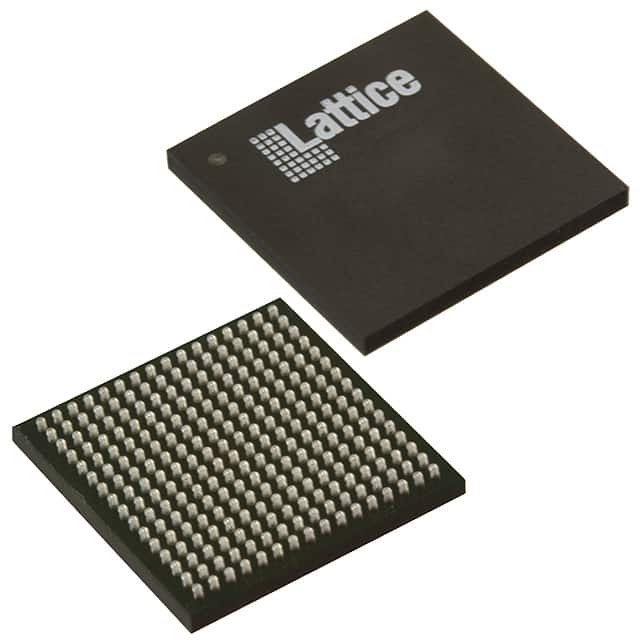
The Lattice Semiconductor LCMXO3LF-1300E-6MG256I is a Field Programmable Gate Array (FPGA) designed for various embedded applications. This device features 1280 logic elements and 160 Look-Up Tables (LUTs), providing a flexible platform for custom logic implementation. It offers 206 Input/Output (I/O) pins, enabling extensive connectivity with other system components.
The FPGA operates within a voltage range of 1.14V to 1.26V and has a total of 65536 RAM bits. The operating temperature range is specified from -40°C to 100°C (TJ), making it suitable for a wide array of environmental conditions. The component is housed in a 256-CSFBGA (9x9) package and utilizes a Surface Mount type for integration onto printed circuit boards.
This FPGA is part of the MachXO3LF family, known for its low power consumption and high performance. Its robust design and comprehensive feature set make it a suitable choice for applications requiring custom digital logic, control functions, and interface bridging. The 256-VFBGA, CSPBGA package ensures a compact footprint for space-constrained designs.
The LCMXO3LF-1300E-6MG256I FPGA has 1280 logic elements.
The LCMXO3LF-1300E-6MG256I FPGA has 206 I/O pins.
The operating voltage for the LCMXO3LF-1300E-6MG256I FPGA is between 1.14V and 1.26V.
The LCMXO3LF-1300E-6MG256I FPGA is available in a 256-VFBGA, CSPBGA package.
The LCMXO3LF-1300E-6MG256I FPGA operates from -40°C to 100°C (TJ).