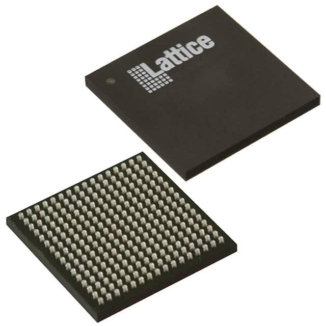
The Lattice Semiconductor LCMXO3L-6900E-6MG256I is a Field Programmable Gate Array (FPGA) designed for various embedded applications. This device features 6864 logic elements and 858 Look-Up Tables (LUTs), providing significant processing capability. It offers 206 input/output (I/O) pins, allowing for extensive interfacing with other components.
The FPGA operates within a voltage range of 1.14V to 1.26V and has a junction temperature operating range of -40°C to 100°C. It includes 245760 total RAM bits for data storage and manipulation. The device is available in a 256-VFBGA, CSPBGA package, suitable for surface mount applications.
This FPGA is designed for applications requiring flexible and reconfigurable logic. Its specifications make it suitable for a range of digital processing tasks where custom hardware acceleration or specific logic functions are needed. The surface mount package facilitates integration into compact electronic designs.