

| Distributor | Stock | Pricing | MOQ | PKG | Lead Time | Date Code | On Order Quantity | On Order Delivery | |
|---|---|---|---|---|---|---|---|---|---|
|
3 pcs
|
3 pcs | On Request | 1 | On Request | On Request | On Request | On Request | On Request |
| Category | |
| Manufacturer Name | |
| Lead Spacing | |
| Mounting Type | |
| Number of I | |
| Number of LABs | |
| Number of Logic Elements | |
| Operating Temperature | |
| Supplier Device Package | |
| Tape & Reel | |
| Total RAM Bits | |
| Voltage |
The Lattice Semiconductor LCMXO3L-2100E-5UWG49ITR1K is a member of the MachXO3 family of FPGAs, designed for ultra-low density applications requiring advanced programmable bridging and I/O expansion. This device features 2112 logic elements and 264 Look-Up Tables (LUTs), providing 75776 total RAM bits for flexible implementation.
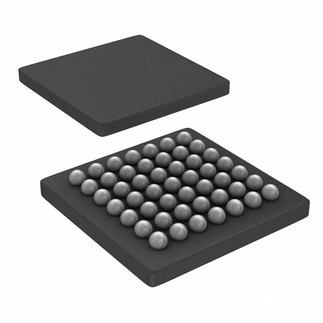
With 38 I/O pins, the LCMXO3L-2100E-5UWG49ITR1K supports a wide range of interfacing capabilities. It operates at a voltage range of 1.14V to 1.26V and has an operating temperature range of -40°C to 100°C (TJ). The device is housed in a compact 49-WLCSP (Wafer Level Chip Scale Package) with surface mount mounting type, making it suitable for space-constrained designs.
This FPGA is designed on a 65nm non-volatile low power process, offering features such as programmable low swing differential I/Os and the ability to dynamically turn off I/O banks, on-chip PLLs, and oscillators to manage power consumption. It is suitable for low-cost, high-volume consumer and system applications.
The LCMXO3L-2100E-5UWG49ITR1K FPGA has 2112 logic elements.
The operating voltage for the LCMXO3L-2100E-5UWG49ITR1K FPGA is between 1.14V and 1.26V.
This FPGA is supplied in a 49-WLCSP (Wafer Level Chip Scale Package).
The operating temperature range is -40°C to 100°C (TJ).
The LCMXO3L-2100E-5UWG49ITR1K features 38 I/O pins.