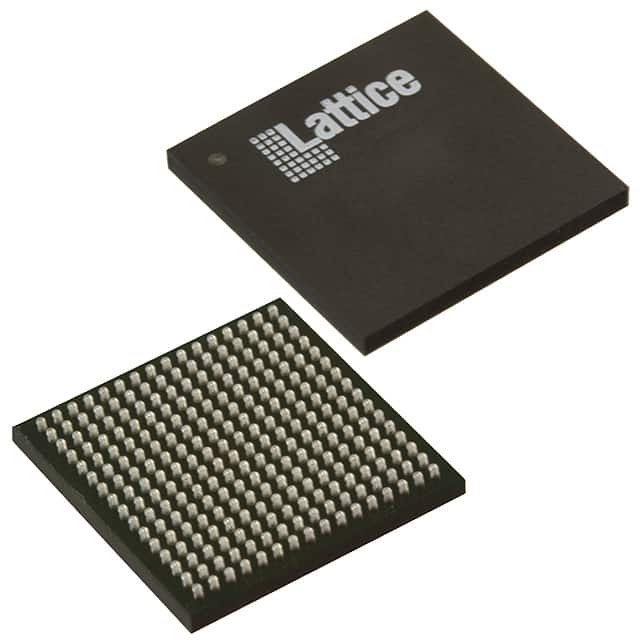
This Lattice Semiconductor LCMXO3L-2100E-5MG256I is a Field Programmable Gate Array (FPGA) designed for various embedded applications. It features 2112 logic elements and 264 LABs, providing significant processing capability.
The device offers 206 I/O pins and 75776 total RAM bits, supporting complex logic functions and data storage. It operates at a voltage range of 1.14V to 1.26V and has an operating temperature range of -40°C to 100°C (TJ).
Packaged in a 256-CSFBGA (9x9) format, this FPGA is designed for surface mounting. Its compact size and robust specifications make it suitable for integration into space-constrained designs.
The LCMXO3L-2100E-5MG256I is RoHS3 compliant, has an MSL of 1, and is REACH unaffected, meeting standard environmental and safety requirements for electronic components.