

| Distributor | Stock | Pricing | MOQ | PKG | Lead Time | Date Code | On Order Quantity | On Order Delivery | |
|---|---|---|---|---|---|---|---|---|---|
|
9,606 pcs
|
9606 pcs | On Request | 1 | On Request | On Request | On Request | On Request | On Request | |
|
89 pcs
|
89 pcs | On Request | 1 | On Request | On Request | 1115 | On Request | On Request |
| Category | |
| Manufacturer Name | |
| Lead Spacing | |
| Memory Size | |
| Mounting Type | |
| Number of I | |
| Number of LABs | |
| Number of Logic Elements | |
| Operating Temperature | |
| Supplier Device Package | |
| Tape & Reel | |
| Voltage |
The Lattice Semiconductor LCMXO256C-5TN100C is a member of the MachXO family of FPGAs, designed for applications such as glue logic, bus bridging, and control logic. This device features 256 LUTs (Look-Up Tables) and provides 78 I/O pins, supporting a wide range of I/O standards including LVCMOS, LVTTL, PCI, LVDS, and others.
With an operating voltage range of 1.71V to 3.465V and an operating temperature range of 0°C to 85°C, the LCMXO256C-5TN100C is suitable for various embedded systems. It includes embedded and distributed memory options, with up to 7.7 Kbits of distributed RAM and 27.6 Kbits of sysMEM™ Embedded Block RAM. The device also supports up to two sysCLOCK™ PLLs for clock management.
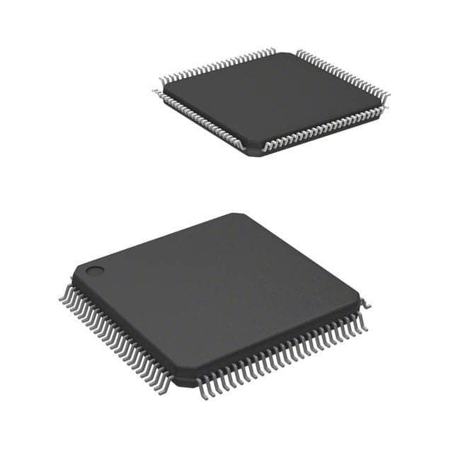
This FPGA is supplied in a 100-TQFP (14x14 mm) package and utilizes Surface Mount technology for integration onto printed circuit boards. It offers features like instant-on capability and non-volatile configuration, making it a versatile solution for CPLD and low-capacity FPGA applications.
The LCMXO256C-5TN100C has 256 logic elements.
The LCMXO256C-5TN100C offers 78 I/O pins.
The operating voltage range for the LCMXO256C-5TN100C is 1.71V to 3.465V.
The LCMXO256C-5TN100C is supplied in a 100-TQFP (14x14 mm) package.
The LCMXO256C-5TN100C supports LVCMOS 3.3/2.5/1.8/1.5/1.2, LVTTL, PCI, LVDS, Bus-LVDS, LVPECL, and RSDS.
Yes, the LCMXO256C-5TN100C has up to 27.6 Kbits of sysMEM™ Embedded Block RAM.