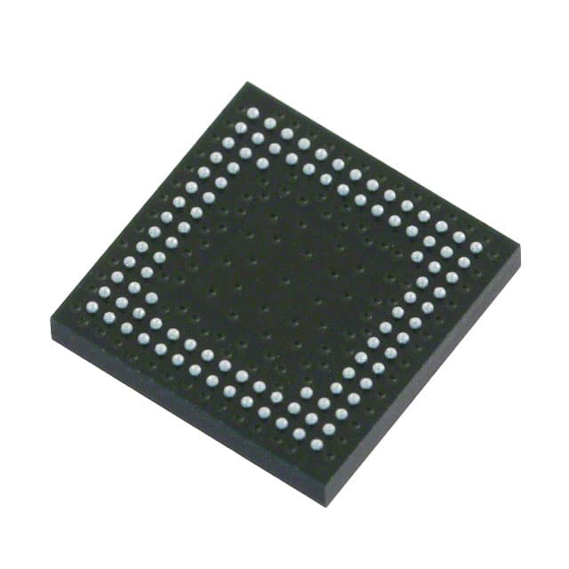
LCMXO256C-3MN100C The Lattice Semiconductor LCMXO256C-3MN100C is an FPGA with 256 LUTs and 78 I/O pins. It operates within a voltage range of 1.71V to 3.465V.
Mfr Part #:

LCMXO256C-3MN100C

Available from 5 distributors
Mfr Name: Lattice Semiconductor Corporation
Lattice Semiconductor Corporation
The Lattice Semiconductor LCMXO256C-3MN100C is an FPGA with 256 LUTs and 78 I/O pins. It operates within a voltage range of 1.71V to 3.465V.
✓ Total Stock: 2,311 pcs

LCMXO256C-3MN100C Available from 5 distributors

✓ Authorised
✓ Non-Authorised

LCMXO256C-3MN100C Specifications Quick View

Most important parameters for selection – full specs in datasheet.
Category
Manufacturer Name
Mounting Type
Number of I
Number of LABs
Number of Logic Elements
Operating Temperature
Supplier Device Package
Voltage

LCMXO256C-3MN100C Description

Short technical summary and product information.

The Lattice Semiconductor LCMXO256C-3MN100C is a non-volatile, infinitely reconfigurable FPGA designed for applications traditionally addressed by CPLDs and low-capacity FPGAs. It offers 256 LUTs and supports 78 I/O pins, making it suitable for glue logic, bus bridging, and control functions.


This device features a flexible I/O buffer supporting various interfaces including LVCMOS, LVTTL, PCI, and LVDS. It also includes embedded and distributed memory, with up to 27.6 Kbits of sysMEM™ Embedded Block RAM and 7.7 Kbits of distributed RAM. The MachXO family supports up to two analog PLLs for clock management.


The LCMXO256C-3MN100C is available in a 100-CSBGA (8x8 mm) surface mount package. It operates within a voltage range of 1.71V to 3.465V and has an operating temperature range of 0°C to 85°C (TJ). The device supports instant-on functionality, powering up in microseconds, and offers excellent design security.


System-level support includes IEEE Standard 1149.1 Boundary Scan and IEEE 1532 compliant in-system programming. The TransFR™ Reconfiguration (TFR) feature allows for in-field logic updates while the system operates.


LCMXO256C-3MN100C Quick Information

Product Type: FPGA
Series: MachXO
Canonical Name: LCMXO256C-3MN100C FPGA
Subcategory: Field Programmable Gate Array

LCMXO256C-3MN100C Compliance

RoHS Status: RoHS Compliant
Moisture Sensitivity Level (MSL): 1 Unlimited
REACH Status: REACH Unaffected
Lead Free: Lead free/RoHS compliant packaging

LCMXO256C-3MN100C Features

  • Non-volatile, infinitely reconfigurable FPGA.
  • 256 LUTs and 78 I/O pins.
  • 1.71V to 3.465V operating voltage range.
  • 100-CSBGA surface mount package.
  • Instant-on functionality, powers up in microseconds.

LCMXO256C-3MN100C Applications

  • Glue logic implementation.
  • Bus bridging and interfacing.
  • Power-up control circuits.
  • Control logic applications.

LCMXO256C-3MN100C FAQs

6 frequently asked questions generated from this part’s specifications.
What is the number of logic elements in the LCMXO256C-3MN100C?

The LCMXO256C-3MN100C has 256 logic elements.

How many I/O pins does the LCMXO256C-3MN100C have?

The LCMXO256C-3MN100C has 78 I/O pins.

What is the operating voltage range for the LCMXO256C-3MN100C?

The operating voltage range for the LCMXO256C-3MN100C is 1.71V to 3.465V.

What package type is the LCMXO256C-3MN100C available in?

The LCMXO256C-3MN100C is available in a 100-CSBGA (8x8 mm) package.

What are the embedded and distributed memory capabilities of the LCMXO256C-3MN100C?

It offers up to 27.6 Kbits of sysMEM™ Embedded Block RAM and up to 7.7 Kbits of distributed RAM.

Does the LCMXO256C-3MN100C support in-field logic updates?

Yes, the LCMXO256C-3MN100C supports in-field logic updates through TransFR™ Reconfiguration (TFR).

LCMXO256C-3MN100C Alternate Parts

Same form/fit/function or matching attribute configuration across different manufacturers.
View All Alternate Parts
LCMXO256C-5MN100C
LCMXO256C-5MN100C
Lattice Semiconductor Corporation
The Lattice Semiconductor LCMXO256C-5MN100C is a MachXO series FPGA featuring 256 logic elements and 78 I/O pins. It operates with a supply voltage range of 1.71V to 3.465V.
View Part
LCMXO256C-4M100C
LCMXO256C-4M100C
Lattice Semiconductor Corporation
The Lattice Semiconductor LCMXO256C-4M100C is a Field Programmable Gate Array (FPGA) with 256 logic elements and 78 I/O pins. It operates within a voltage range of 1.71V to 3.465V.
View Part
LCMXO256C-4MN100C
LCMXO256C-4MN100C
Lattice Semiconductor Corporation
IC FPGA 78 I/O 100CSBGA
View Part
LCMXO256C-3M100C
LCMXO256C-3M100C
Lattice Semiconductor Corporation
IC FPGA 78 I/O 100CSBGA
View Part
Home
Account

Categories