

| Distributor | Stock | Pricing | MOQ | PKG | Lead Time | Date Code | On Order Quantity | On Order Delivery | |
|---|---|---|---|---|---|---|---|---|---|
|
1,500 pcs
|
1500 pcs | On Request | 1 | On Request | On Request | On Request | On Request | On Request |
| Category | |
| Manufacturer Name | |
| Lead Spacing | |
| Mounting Type | |
| Number of I | |
| Number of LABs | |
| Number of Logic Elements | |
| Operating Temperature | |
| Operating Voltage | |
| Supplier Device Package | |
| Total RAM Bits | |
| Voltage |
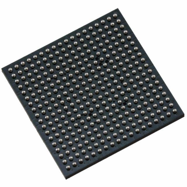
The Lattice Semiconductor LCMXO2280E-3FTN324C is a Field Programmable Gate Array (FPGA) belonging to the MachXO family. This device is designed for applications requiring flexible logic implementation and high I/O density.
Key specifications include 2280 logic elements and 285 LABs/CLBs, providing substantial capacity for complex designs. It features 271 general-purpose I/O pins, enabling extensive connectivity. The integrated memory includes 28,262 bits of RAM for high-speed data buffering.
The device operates within a supply voltage range of 1.14V to 1.26V and has an operating temperature range of 0°C to 85°C (TJ). It is supplied in a 324-FTBGA package, suitable for surface mounting.
This FPGA is optimized for applications such as glue logic, bus bridging, and control functions, offering a balance of performance and density for embedded systems.
The LCMXO2280E-3FTN324C has 2280 logic elements.
The LCMXO2280E-3FTN324C provides 271 I/O pins.
The operating voltage range for the LCMXO2280E-3FTN324C is 1.14V to 1.26V.
The LCMXO2280E-3FTN324C is supplied in a 324-FTBGA package.
The operating temperature range is 0°C to 85°C (TJ).
The LCMXO2280E-3FTN324C has 28,262 bits of embedded RAM.