

| Distributor | Stock | Pricing | MOQ | PKG | Lead Time | Date Code | On Order Quantity | On Order Delivery | |
|---|---|---|---|---|---|---|---|---|---|
|
5,500 pcs
|
5500 pcs | On Request | 1 | On Request | On Request | On Request | On Request | On Request |
| Category | |
| Manufacturer Name | |
| Lead Spacing | |
| Mounting Type | |
| Number of I | |
| Number of LABs | |
| Number of Logic Elements | |
| Operating Temperature | |
| Supplier Device Package | |
| Total RAM Bits | |
| Voltage |
The Lattice Semiconductor LCMXO2280E-3FTN256I is a Field Programmable Gate Array (FPGA) from the MachXO series. It offers 2280 logic elements and 285 LABs/CLBs, providing moderate logic density suitable for control, interfacing, and basic datapath tasks.
This FPGA features 211 general-purpose I/O pins, enabling extensive connectivity. It includes 28,262 bits of embedded RAM for high-speed data buffering. The device operates within a supply voltage range of 1.14V to 1.26V and has an operating junction temperature range of -40°C to 100°C.
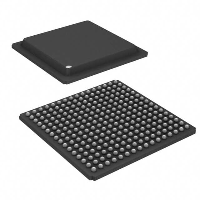
The LCMXO2280E-3FTN256I is housed in a 256-ball Fine-Pitch Thin Ball Grid Array (FTBGA) package, measuring 17x17 mm, designed for surface mounting. This package facilitates dense PCB mounting and offers high pin count for design flexibility. The device is classified with ECCN 3A991D.
The LCMXO2280E-3FTN256I FPGA has 2280 logic elements and 285 LABs/CLBs.
The LCMXO2280E-3FTN256I FPGA features 211 general-purpose I/O pins.
The supply voltage range for the LCMXO2280E-3FTN256I FPGA is 1.14V to 1.26V.
The LCMXO2280E-3FTN256I FPGA is supplied in a 256-FTBGA (17x17 mm) package and a 256-LBGA package.
The operating junction temperature range for the LCMXO2280E-3FTN256I FPGA is -40°C to 100°C.
The ECCN for the LCMXO2280E-3FTN256I FPGA is 3A991D.