

| Distributor | Stock | Pricing | MOQ | PKG | Lead Time | Date Code | On Order Quantity | On Order Delivery | |
|---|---|---|---|---|---|---|---|---|---|
|
817 pcs
|
817 pcs | On Request | 1 | On Request | On Request | On Request | On Request | On Request |
| Category | |
| Manufacturer Name | |
| Mounting Type | |
| Number of I/O | |
| Supplier Device Package | |
| Voltage |
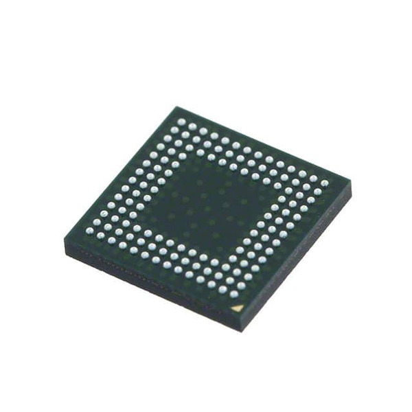
The LCMXO2280C-5FTN324C-4I is a Field Programmable Gate Array (FPGA) Integrated Circuit (IC) from Lattice Semiconductor, designed for embedded applications. This device belongs to the MachXO family, offering flexible logic implementation, device interfacing, and customizable hardware functions.
Key specifications include 101 input/output pins, providing versatile connectivity for various application requirements. It features 2280 logic elements/cells and 285 Logic Array Blocks/Configurable Logic Blocks (LABs/CLBs), offering adequate programmable resources for mid-range complexity designs. The total RAM available is 28,262 bits, suitable for moderate data storage needs in logic operations and memory management.
The operating voltage ranges from 1.71V to 3.465V, and it operates within a temperature range of 0°C to 85°C (TJ). The IC is supplied in a 132-ball CSPBGA surface-mount package, specifically a 132-LFBGA, CSPBGA type.
This FPGA IC provides programmable logic for system designers seeking cost-effective, low-power, and reliable programmable solutions. Its primary function is to enable customizable hardware functions and efficient device interfacing.
| Qty | Low | High |
|---|---|---|
| 1+ | $4.72 | $4.72 |
Estimated market price range - modelled values for guidance only, not live distributor offers.
The operating voltage range is 1.71V to 3.465V.
The operating temperature range is 0°C to 85°C.
It is supplied in a 132-LFBGA, CSPBGA package.
This FPGA IC has 2280 logic elements/cells.
The total RAM available is 28,262 bits.
The LCMXO2280C-5FTN324C-4I features 101 input/output pins.