
LCMXO2280C-5MN132C
Lattice Semiconductor Corporation
The Lattice LCMXO2280C-5MN132C is a MachXO family FPGA with 2280 LUTs and 101 I/O pins. It supports a wide range of interfaces and operates from 1.71V to 3.465V.


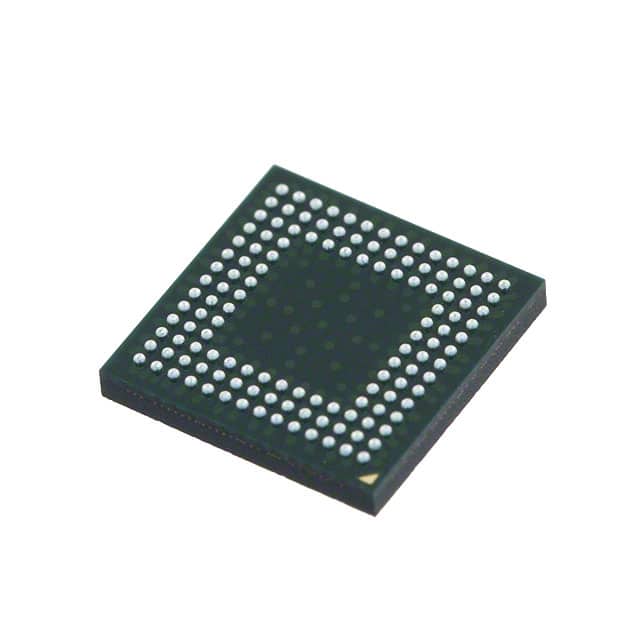
| Distributor | Stock | Pricing | MOQ | PKG | Lead Time | Date Code | On Order Quantity | On Order Delivery | |
|---|---|---|---|---|---|---|---|---|---|
|
1,609 pcs
|
1609 pcs | On Request | 1 | On Request | On Request | On Request | On Request | On Request | |
|
675 pcs
|
675 pcs | On Request | 1 | On Request | On Request | On Request | On Request | On Request |
| Category | |
| Manufacturer Name | |
| Mounting Type | |
| Number of I | |
| Number of LABs | |
| Number of Logic Elements | |
| Operating Temperature | |
| Supplier Device Package | |
| Tape & Reel | |
| Total RAM Bits | |
| Voltage |
The Lattice FPGA model LCMXO2280C-3MN132C is a programmable logic device designed for embedded systems. It contains 2280 logic elements and 285 logic array blocks, providing substantial logic capacity for complex digital designs. The device includes 28.262 Kbits of total RAM and supports up to 101 I/O pins, enabling versatile interfacing options.
This FPGA operates within a voltage range of 1.71V to 3.465V and is mounted using a surface-mount package, specifically a 132-ball CSBGA. It supports a variety of programmable I/O standards, including LVCMOS, LVTTL, PCI, LVDS, Bus-LVDS, LVPECL, and RSDS. The device features two PLLs for clock management and non-volatile configuration memory, allowing for reconfiguration without losing programmed data. Programming is performed via JTAG interface, facilitating in-system programming.
Designed for embedded applications, this FPGA is suitable for digital signal processing, communication, and control systems requiring high logic density and flexible I/O options.
The device contains 2280 logic elements.
The FPGA supports 101 I/O pins.
The device operates within 1.71V to 3.465V.
It uses a 132-ball CSBGA surface mount package.